


180
Chapter 12 Instruction Cache
2.Main body structure
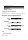
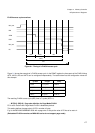
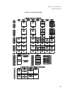
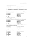
Figure 2-2 Instruction Cache Tag
[Bits 31 to 9] Address tag
This area stores the upper 23 bits of the memory address of the instruction cached in the
corresponding block. For example, memory address IA of the instruction data stored in sub-
block k in block i is obtained from the following equation:
IA = address tag x 2
11
+ i x 2
4
+ k x 2
2
The address tag is used to check for a match with the instruction address requested for
access by the CPU. The CPU and cache behave as follows depending on the result of the
cache check:
1) When the requested instruction data exists in the cache (hit), the cache transfers the data
to the CPU within the cycle.
2) When the requested instruction data does not exist in the cache (miss), the CPU and
cache obtain the data loaded by external access at the same time.
[Bits 7 to 4] SBV3 to SBV0: Sub-block valid bits
When SBV* contains "1", the corresponding sub-block holds the current instruction data at
the address located by the tag. Each sub-block usually holds two instructions (including
immediate-value transfer instructions).
[Bit 3] TAGV: TAG valid bit
This bit indicates whether the address tag value is valid. When the bit contains "0", the
corresponding block is invalid regardless of the settings of the sub-block validation bits. (The
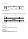
Address tag Reserved
ETLKLRUReservedTAGVSBV0SBV1SBV2SBV3
Way 1
0809
07 0506 0304 01 0002
31
Sub-block valid
LRU
Entry lock
TAG valid
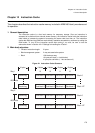
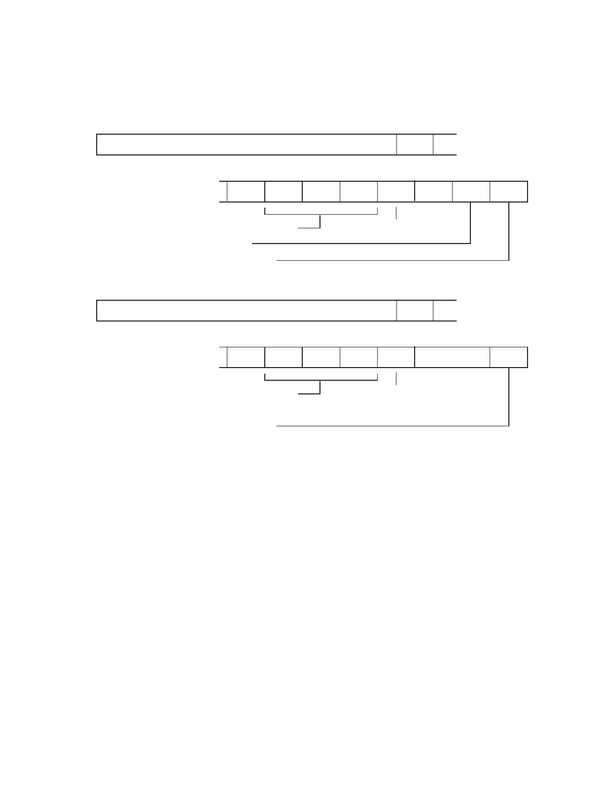
Address tag Reserved
ETLKReservedTAGVSBV0SBV1SBV2SBV3
Way 2
0809
07 0506 0304 01 0002
31
Sub-block valid
Entry lock
TAG valid