


218
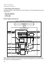
Chapter 15 CAN Clock Prescaler
3.Registers
3. Registers
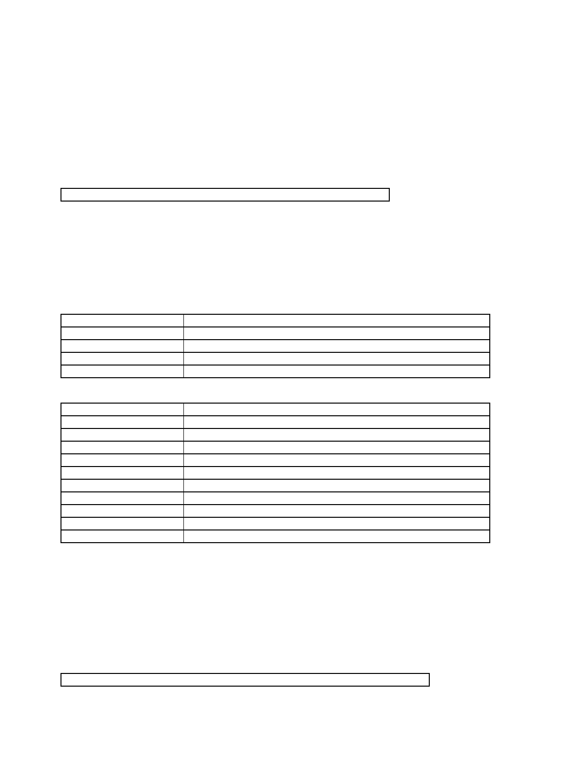
3.1 CAN Clock Control Register
Controls the CAN clock source, the clock division ratio and the clock disable.
• CANPRE: Address 04C0h (Access: Byte)
(See “Meaning of Bit Attribute Symbols (Page No.10)” for details of the attributes.)
• Bit7-6: Reserved bitAlways write “0” to these register bits.
• Bit5-4: CAN Prescaler ClocK Selection
• Bit3-0: Source clock Divide-by-C selection
(Note) Do not exceed the specified upper frequency limit of CANCLK (e.g. 20 MHz) e.g. by setting prescaler
values exceeding this limit, or by switching the prescaler clock source to a higher frequency clock
without switching previously the prescaler values to higher division rates.
(Note) If prescaler source is selected to PLL output: Even though it is possible to select no division ratio (:1)
for the divide-by-C counter it is not recommended. The resulting output clock will have an odd clock
duty ratio (direct PLL output can have up to 90:10 duty). Always select at least a division ratio > 1.
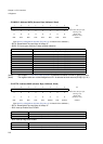
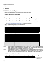
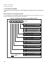
• CANCKD: Address 04C1h (Access: Byte)
76543210 bit
- - CPCKS1 CPCKS0 DVC3 DVC2 DVC1 DVC0
00000000
Initial value (INITpin input,
watchdog reset
)
00XXXXXX
Initial value
(Software reset)
R0/W0 R0/W0 R/W R/W R/W R/W R/W R/W Attribute
CPCKS1-CPCKS0 Prescaler clock source
00 CLKB, core clock (inital)
01 PLL output
10 reserved
11 Main oscillation
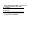
DVC3-DVC0 Source clock divided-by-C (generates CANCLK)
0000 Source clock : 1 (no division)
0001 Source clock : 2 (division by 2)
0010 Source clock : 3 (division by 3)
0011 Source clock : 4 (division by 4)
0100 Source clock : 5 (division by 5)
0101 Source clock : 6 (division by 6)
0110 Source clock : 7 (division by 7)
0111 Source clock : 8 (division by 8)
...... .....
1111 Source clock : 16 (division by 16)
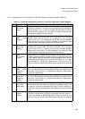
76543210 bit
- - CANCKD5 CANCKD4 CANCKD3 CANCKD2 CANCKD1 CANCKD0
00000000
Initial value (
INIT pininput,
watchdog reset)