


929
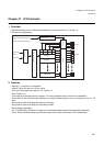
Chapter 47 LCD Controller
5.Operation
5. Operation
This section describes operation.
5.1 LCD Controller/Driver (LCDC) Operation
(1) Set values to the display data memory (VRAM) in advance.
(2) Make necessary settings to each register.
(3) When the frame period generation clock oscillates, LCD drive waveform is output through common/
segment output pins (COM0 - COM3, SEG0 - SEG39).
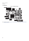
(4) More detailedly,
VRAM contents are automatically read in synchronization with common signals to be output through
segment output pins.
(If the bit is set to “1”, the selected waveform is output through the segment output pins.
If the bit is set to “0”, non-selected waveform is output through the segment output pins.)
If the display mode is set to 1/2 duty cycle, non-selected waveform is output through the COM2 and
COM3 pins. For the 1/3 duty cycle, the COM3 pin is used to output non-selected waveform.
(5) This output waveform is a 2-frame AC waveform in accordance with the duty cycle setting, and drives
LCD.
(6) When MS[1:0] = “00” is used to deactivate LCD, a “L” level is output through both common and segment
pins.
(7) If LCD operation is enabled in the sub-stop mode (LCEN=“1”), LCD display is displayed.
Note that frame period generation clock signals must be supplied at this time.
(8) LCD display can be blanked by selecting “blank” (BK=“1”) in blanking selection.
Note that non-selected waveform continues to be output.
(9) When LCD deactivation (MS[1:0]=“00”) is selected with the display mode, LCD ceases to operate.
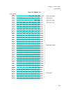
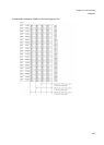
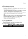
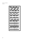
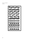
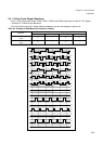
5.2 1/2 Duty Cycle Output Waveform
Only COM0 and COM1 outputs are used for LCD display. Neither COM2 nor COM3 output is used.
• Example of 1/3 Bias Output Waveform
LCD cells with the maximum voltage difference between common and segment outputs are lit.
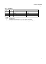
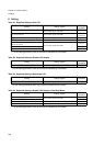
Table 5-1 Example of Data Memory Contents for display
Segment
Contents of data memory for display
COM3 output COM2 output COM1 output COM0 output
SEG 2n output - - 0 0
SEG2n+1 output - - 0 1