


618
Chapter 32 USART (LIN / FIFO)
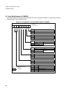
2.USART Configuration
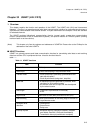
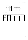
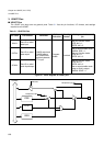
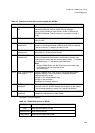
• Reception Data Register
This register retains reception data. Serial input data is converted and stored in this register. If the FIFO is
enabled up to 16 receptions can be saved, the trigger level is progammable.
• Transmission Control Circuit
The transmission control circuit consists of a transmission bit counter, transmission start circuit, and
transmission parity counter.The transmission bit counter counts transmission data bits. When the transmission
of one data item of the specified data length is complete, the transmission bit counter sets the Transmission
data register full flag. The transmission start circuit starts transmission when data is written to TDR04. The
transmission parity counter generates a parity bit for data to be transmitted if parity is enabled.
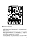
• Transmission Shift Register
The transmission shift register transfers data written to the TDR04 register to itself and outputs the data to the
SOT04 pin, shifting the data bit by bit.
• Transmission Data Register
This register sets transmission data. Data written to this register is converted to serial data and output.
If the FIFO is enabled up to 16 transmissions can be saved and continuously transmitted
• Error Detection Circuit
The error detection circuit checks if there was any error during the last reception. If an error has occurred it
sets the corresponding error flags.
• Oversampling Unit
The oversampling unit oversamples the incoming data at the SIN04 pin for five times. It is switched off in
synchronous operation mode.
• Interrupt Generation Circuit
The interrupt generation circuit administers all cases of generating a reception or transmission interrupt. If a
corresponding enable flag is set and an interrupt case occurs the interrupt will be generated immediately.
• LIN Break and Synchronization Field Detection Circuit
The LIN break and LIN synchronization field detection circuit detects a LIN break, if a LIN master node is
sending a message header. If a LIN break is detected a special flag bit is generated. The first and the fifth
falling edge of the synchronization field is recognized by this circuit by generating an internal signal for the
Input Capture Unit to measure the actual serial clock time of the transmitting master node.
• LIN Break Generation Circuit
The LIN break generation circuit generates a LIN break of a determined length.
• Bus Idle Detection circuit
The bus idle detection circuit recognizes if neither reception nor transmission is going on. In this case the
circuit generates a special flag bit.
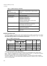
• Serial Mode Register
This register performs the following operations:
• Selecting the USART operation mode
• Selecting a clock input source
• Selecting if an external clock is connected “one-to-one” or connected to the reload counter
• Resetting the USART (preserving the settings of the registers)
• Specifying whether to enable serial data output to the corresponding pin
• Specifying whether to enable clock output to the corresponding pin
• Serial Control Register
This register performs the following operations:
• Specifying whether to provide parity bits
• Selecting parity bits
• Specifying a stop bit length