


190
Chapter 13 Clock Control
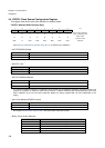
3.Configuration
• External bus clock (CLKT): F/1, /2, /3, /4, /5, /6, /7, /8, ..., /16
The clock used by the external bus expansion interface. The circuits that use this clock are as follows.
• External bus expansion interface
• External CLK output
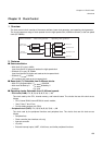
3. Configuration
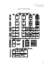
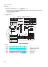
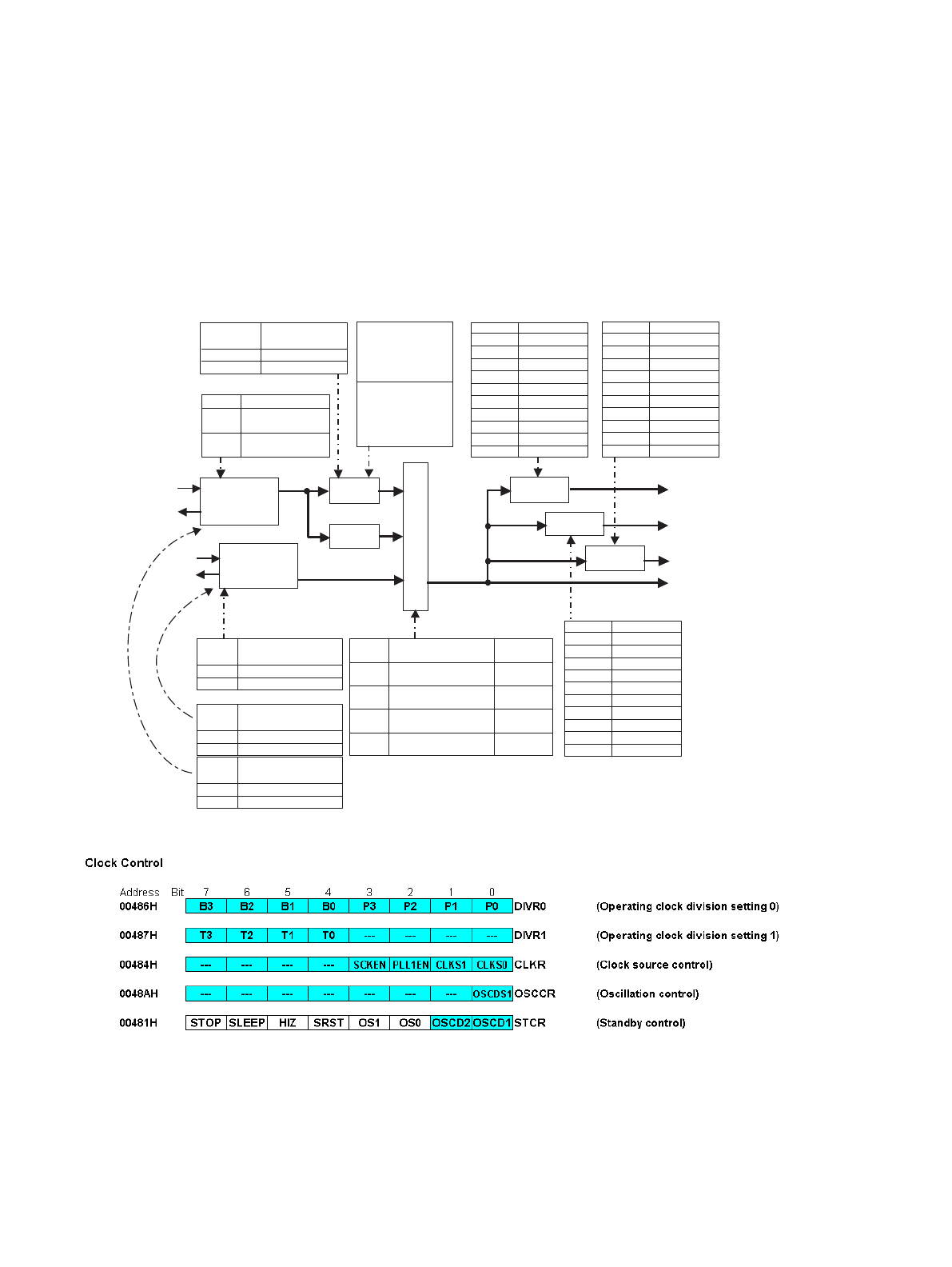
Figure 3-1 Configuration Diagram
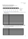
Figure 3-2 Register List
Selector
Divider
Main clock
source
Subclock
source
(F
CLK-MAIN
)
(F
CLK-SUB
)
Divide by 2
PLL
Divider
Divider
CPU clock
(F
CLK B
)
Peripheral clock
(F
CLK P
)
External bus clock
(F
CLK T
)
Base
clock
(φ)
(φ)
Base clock
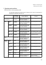
B3-B0
0000
0001
0010
0011
0100
0101
0110
0111
1000-1110
1111
DIVR0: bit 7-4
No division
Divide by 2
Divide by 3
Divide by 4
Divide by 5
Divide by 6
Divide by 7
Divide by 8
Divide by 9-15
Divide by 16
PLL1EN
0
1
CLKR: bit2
Halt PLL
Enable (start) PLL
SCKEN
0
1
CLKR: bit3
Subclock selection prohibited
Subclock selection enabled
OSCDS1
0
1
OSCCR: bit0
Main clock continues to
run in subclock mode
Main clock halts in
subclock mode
X0
X1
X1A
X0A
(F
CLK T
)
CLKS1-
CLKS0
CLKR: bit6-4
Permitted
change
00
01
10
11
Main clock divided by 2
(main clock mode)
Main clock divided by 2
(main clock mode)
Main PLL
(main clock mode)
Subclock
(subclock mode)
00=>01, 10
01=>11, 00
10=>00
11=>01
OSCD2
0
1
STCR: bit1
Continue oscillation in stop mode
Halt oscillation in stop mode
Set PLL multiplier
PLLDIVM: bit5-0
PLLDIVN: bit5-0
Set PLL autogear
PLLDIVG: bit5-0
PLLMULG: bit7-0
T3-T0
0000
0001
0010
0011
0100
0101
0110
0111
1000-1110
1111
DIVR1: bit 7-4
No division
Divide by 2
Divide by 3
Divide by 4
Divide by 5
Divide by 6
Divide by 7
Divide by 8
Divide by 9-15
Divide by 16
P3-P0
0000
0001
0010
0011
0100
0101
0110
0111
1000-1110
1111
DIVR1: bit3-0
No division
Divide by 2
Divide by 3
Divide by 4
Divide by 5
Divide by 6
Divide by 7
Divide by 8
Divide by 9-15
Divide by 16
OSCD1
0
1
STCR: bit0
Continue oscillation in stop mode
Halt oscillation in stop mode