


410
Chapter 29 MPU / EDSU
4.Registers
4.2 Explanations of Registers
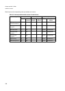
● EDSU Control Register (BCTRL)
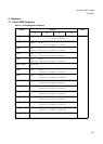
Default Permission Register
The default permission register defines the lowest priority access permissions for the whole memory and I/O ad-
dress range of the MCU. Lowest priority means, that the default permissions take effect for all address regions,
which are NOT covered by any dedicated channel configuration, operating in MPU mode. Default read, write and
execute permissions could be defined for the super visior mode (SV=1) and the normal user mode (SV=0). The su-
per visor mode (SV) is indicated by bit 6 of the CCR in the program status word of the CPU. After the INIT condition
all permissions are set (access allowed).
BIT[15]: SR - Super visor default Read permission register
BIT[14]: SW - Super visor default Write permission register
BIT[13]: SX - Super visor default eXecute permission register
BIT[12]: UR - User default Read permission register
0 Super visor is not permitted to read data
1 Super visor is permitted to read data (default)
0 Super visor is not permitted to write data
1 Super visor is permitted to write data (default)
0 Super visor is not permitted to execute code
1 Super visor is permitted to execute code (default)
0 User is not permitted to read data
1 User is permitted to read data (default)
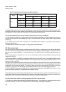
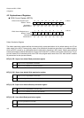
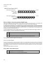
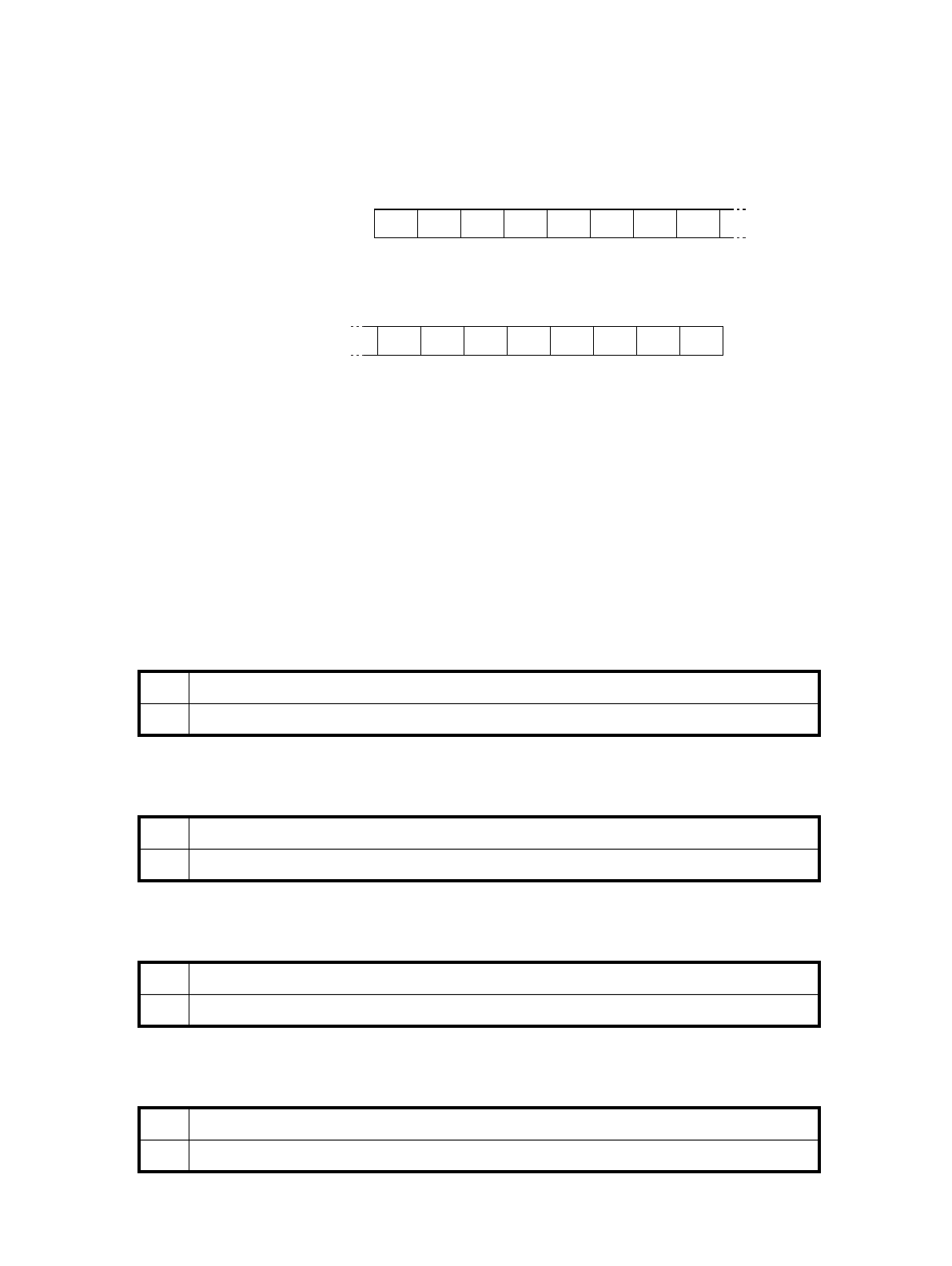
SR SW SX UR UW UX FCPU FDMA
⇐ Bit no.
Read/write ⇒
(R/W) (R/W) (R/W) (R/W) (R/W) (R/W) (R/W) (R/W)
Default value⇒
(1) (1) (1) (1) (1) (1) (0) (0)
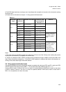
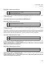
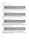
EDSU Control Register byte 2
Address : F002
H
15 14 13 12 11 10 9 8
EEMM PFD SINT1 SINT0 EINT1 EINT0 EINTT EINTR
⇐ Bit no.
Read/write ⇒
(R/W) (R
/W
)(R
/W
)(R
/W
) (R/W) (R/W) (R/W) (R/W)
Default value⇒
(0) (0) (0) (0) (0) (0) (0) (0)
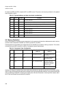
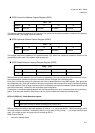
Address :
F0
03H
765432 10
EDSU Control Register byte 3