


400
Chapter 29 MPU / EDSU
3.Break Functions
Break occurs at 0x02345200 to 0x02345300,or
at 0x12345200 to 0x12345300,or
at 0x22345200 to 0x22345300, etc.
The resulting setting of the BD[1:0] status bits indicates the point, respective the area in which the break has oc-
cured.
In the instruction address break mode the following important point has to be considered:
To precisely determine the instruction address where a break occurs, use the PC value saved on the stack during
entry to the instruction break interrupt service routine.
3.2 Operand address break
The operand break function causes a break for the data access address which can be specified by the the operand
address break registers BAD[3:0]. Setting the CTC[1:0] bits of the control register BCR0 to ’01’ provides this mode.
The bits EP[3:0] in BCR0 enable the break points.
Up to 4 breakpoints from channels 0 to 3 can be set. All operand break events are ORed into a operand break ex-
ception interrupt request to the CPU.
For the address mask function the same applies, what is stated in section 3.1 for the Instruction Address Break.
Example: CTC 01 Type: Operand Address Break
EP1 1 Enable break point address BAD1
EM0 1 Set mask BAD0 for break address BAD1
BAD1 0x12345678 Set break address
BAD0 0x00000FFF Set break mask
Break occurs at 0x12345000 to 0x12345FFF
On break at BAD[3:0] the respective flags BD[3:0] in the break interrupt request register BIRQ will be set to ’1’. They
have to be reset by software in the operand break exception routine.
Channels 0 and 1 (BAD0, BAD1) can be set up to function as address range match. Setting the ER0 bit of the control
register BCR0 to ’1’ provides this mode. BAD0 is the lower address and BAD1 is the upper address for address
comparison. In this mode the mask register BAD2 will mask both channels 0 and 1, if the mask feature is enabled
by EM0 = ’1’.
Alternatively channels 2 and 3 (BAD2, BAD3) can be set up to function as address range match. Setting the ER1
bit of the control register BCR0 to ’1’ provides this mode. BAD2 is the lower address and BAD3 is the upper address
for address comparison. In this mode the mask register BAD0 will mask both channels 2 and 3, if the mask feature
is enabled by EM1 = ’1’.
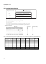
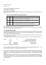
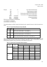
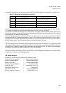
Table 3-1 Instruction Break Detection Status Bits (BD)
BD1 BD0
0 1 Match on point (instruction address == 0x12345200), or
Match on point (instruction address == 0x22345200), etc
1 0 Match on point (instruction address == 0x12345300), or
Match on point (instruction address == 0x22345300), etc
1 1 Match on range (0x12345200 < instruction address < 0x12345300), or
Match on range (0x22345200 < instruction address < 0x22345300), etc