


144
Chapter 9 Reset
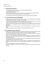
4.Registers
4.3 MOD: Mode Pins
These pins specify the location of the mode vector and reset vector that are read after the MCU is
reset.
4.4 Mode Vector
The data written to the mode register (MODR) by the mode vector fetch operation is called the
mode data. (The mode register is an internal register and cannot be written to or read from
directly.)
After the mode register is set, the MCU operates in accordance with the modes (bus mode and
access mode) set in this register.
The mode data is set by all types of reset. Setting the mode data from the user program is not
possible.
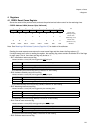
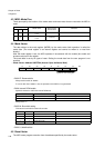
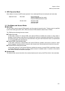
• Mode Vector: Address 000FFF8h (Access: Byte, Half-word, Word)
• Bit32-27: Reserved bits
Always set these bits to “00000”.
If a value other than “00000” is set, the operation of the MCU is not guaranteed.
• Bit26: Internal ROM enable
Specifies whether to enable the internal ROM area.
Always set to “1”.
• Bit25-24: Bus width setting
This sets the bus width for external bus mode.
• Bit23-0: Undefined bits
4.5 Reset Vector
The MCU starts program execution from the address specified by the mode vector.
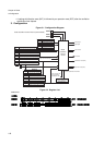
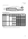
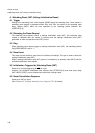
Mode pins
Mode name
Reset vector
Access area
Remarks
MD2 MD1 MD0
00 0
Internal ROM mode
vector
Internal
00 1
External ROM mode
vector
External
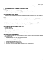
ROMA Function Remarks
0 External ROM mode Enables the external ROM area.
1 Internal ROM mode Enables the internal ROM area.
WTH1 WTH0 Function Remarks
0 0 8-bit bus width
0 1 16-bit bus width
1 0 32-bit bus width
1 1 Single chip mode
31 30 29 28 27 26 25 24 Bit
0 0 0 0 0 ROMA WTH1 WTH0
Operation mode setting bits