


1
Chapter 1 Introduction
1.How to Handle the Device
Chapter 1 Introduction
1. How to Handle the Device
■ Device Handling Instructions
This chapter describes latch-up prevention and pin termination.
● To set latch-up prevention
Latch up may occur on CMOS ICs when the applied voltage for input terminals or output terminals is higher than V
CC
or lower than V
SS
, or a voltage higher than the maximum rating voltage is applied between V
CC
and V
SS
. Make sure
not to apply a voltage higher than the maximum rating voltage since latch up may surge electric current and result in
the thermal destruction of the device.
● Termination of unused pin
An unused pin must be terminated by a pull-up or pull-down resistor externally, or by switching on the internal pull-up
or pull-down resistor before enabling the pin inputs to avoid transverse current.
● Power-supply pin
If multiple V
CC
and V
SS
exist, as a matter of device design, they are connected to each other to prevent an error when
their voltage should be identical in the device. In order to reduce unnecessary radiation, prevent an strobe signal error
due to upward ground level, and comply with total output current standard, be sure to externally connect them to power
supply and ground. Give consideration to connect V
CC and
V
SS
of the device from power supply at low impedance.
Near the device, it is preferable to connect about 0.1uF ceramic capacitor as a bypass capacitor between V
CC
and
V
SS
.
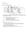
● Crystal-oscillator circuit
Noise to X0 or X1 pin may cause an error. Make a design for printed board to closely allocate X0, X1, crystal oscillator
(or ceramic oscillator), bypass capacitor towards ground and the device.
It is recommended to make a printed board artwork which surrounds X0 and X1 pins using ground.
The above recommendations also apply to the subclock oscillator pins X0A and X1A.
● NC and OPEN pin termination
Do not terminate NC pin and OPEN pin to use.
● Mode pins (from MD0 to MD2)
Connect pins from MD0 to MOD2 directly to V
CC
or V
SS
to use. To avoid entering test mode due to noise, make a short
pattern length between each mode pin on printed board and V
CC
or V
SS
to connect pins at low impedance.
● At the time of power-on
Immediately after power-on operation, be sure to reset INIT pin to initialize the setting (INIT). Immediately after power-
on operation, to ensure the oscillation stabilization time required for oscillation circuit, hold “L”-level input to the pin
during the oscillation stabilization time required for oscillation circuit. (INIT operation on the pin initializes the setting for
oscillation stabilization time to minimum value.)
● Source oscillation input at the time of power-on
At the time of power-on, be sure to input the clock until the oscillation stabilization wait is over.