


444
Chapter 30 I/O Ports
1.I/O Ports Functions
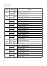
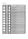
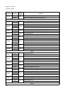
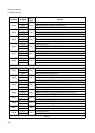
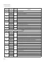
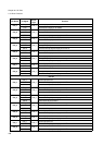
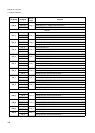
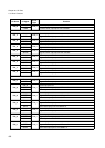
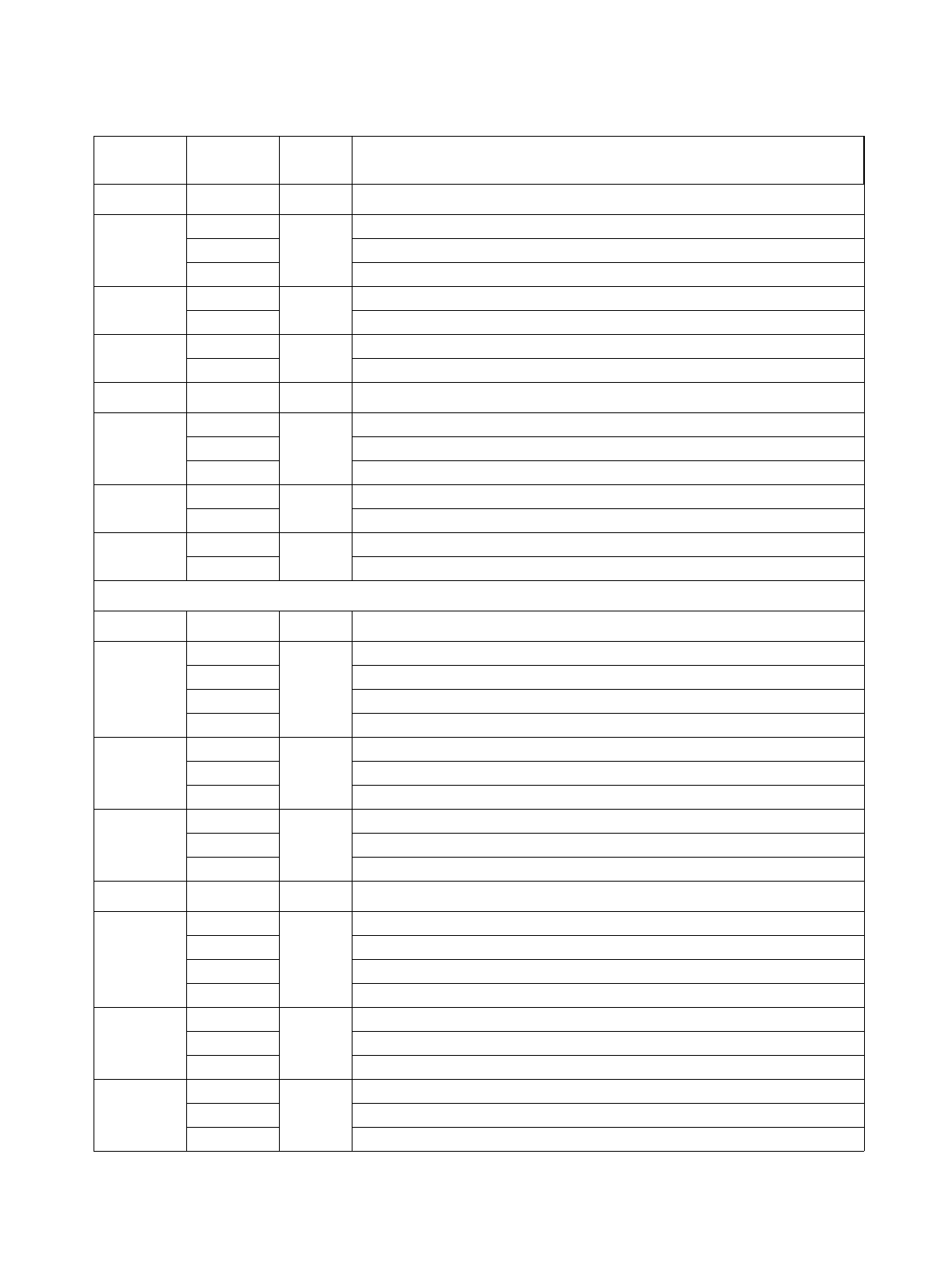
P19_7 P19_7 TP00_0 General purpose I/O.
P19_6
P19_6
TP00_0
General purpose I/O.
SCK5 Clock I/O pin for LIN-USART 5.
CK5 Input for the 16-bit I/O Timer FRT 5.
P19_5
P19_5
TP00_0
General purpose I/O.
SOT5 Serial data output pin for LIN-USART 5.
P19_4
P19_4
TP00_0
General purpose I/O.
SIN5 Serial data input pin for LIN-USART 5.
P19_3 P19_3 TP00_0 General purpose I/O.
P19_2
P19_2
TP00_0
General purpose I/O.
SCK4 Clock I/O pin for LIN-USART 4.
CK4 Input for the 16-bit I/O Timer FRT 4.
P19_1
P19_1
TP00_0
General purpose I/O.
SOT4 Serial data output pin for LIN-USART 4.
P19_0
P19_0
TP00_0
General purpose I/O.
SIN4 Serial data input pin for LIN-USART 4.
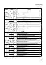
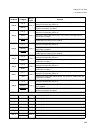
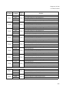
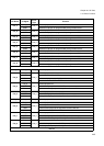
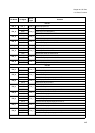
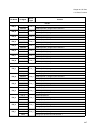
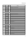
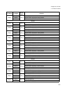
Port 20
P20_7 P20_7 TP00_0 General purpose I/O.
P20_6
P20_6
TP00_0
General purpose I/O.
SCK3 Clock I/O pin for LIN-USART 3.
ZIN1 8-bit reset input pin of the Up-/Down Counter UDC 0/1.
CK3 Input for the 16-bit I/O Timer FRT 3.
P20_5
P20_5
TP00_0
General purpose I/O.
SOT3 Serial data output pin for LIN-USART 3.
BIN1 8-bit down-count input pin of the Up-/Down Counter UDC 0/1.
P20_4
P20_4
TP00_0
General purpose I/O.
SIN3 Serial data input pin for LIN-USART 3.
AIN1 8-bit up-count input pin of the Up-/Down Counter UDC 0/1.
P20_3 P20_3 TP00_0 General purpose I/O.
P20_2
P20_2
TP00_0
General purpose I/O.
SCK2 Clock I/O pin for LIN-USART 2.
ZIN0 8/16-bit reset input pin of the Up-/Down Counter UDC 0/1.
CK2 Input for the 16-bit I/O Timer FRT 2.
P20_1
P20_1
TP00_0
General purpose I/O.
SOT2 Serial data output pin for LIN-USART 2.
BIN0 8/16-bit down-count input pin of the Up-/Down Counter UDC 0/1.
P20_0
P20_0
TP00_0
General purpose I/O.
SIN2 Serial data input pin for LIN-USART 2.
AIN0 8/16-bit up-count input pin of the Up-/Down Counter UDC 0/1.
Pin Name I/O Signal
Circuit
Type
Function