


169
Chapter 11 Memory Controller
8.Explanations of Registers
8. Explanations of Registers
● FLASH Interface Control Register
FLASH Memory Control and Status Register (FMCS)
• BIT[31]: ASYNC - ASYNChronous access enable
The ASYNC bit is cleared at reset, which enables the fast synchronous FLASH access mode by default. To switch
to asynchronous mode, set this bit (however it is basically not recommended to set this bit, neither in read nor in
write access).
• BIT[30]: FIXE - FIXed reset and mode vector Enable
The FIXE bit is set by default.
To enable FLASH access on address 0x000ffff8 and 0x000ffffc, clear this bit.
0 Synchronous FLASH access (default)
1 Asynchronous FLASH access
0 Disable FMV/FRV and enable FLASH access at mode vector address
1 Output the fixed mode or reset vector at address hit (default)
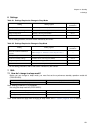
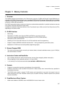
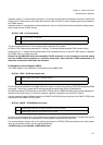
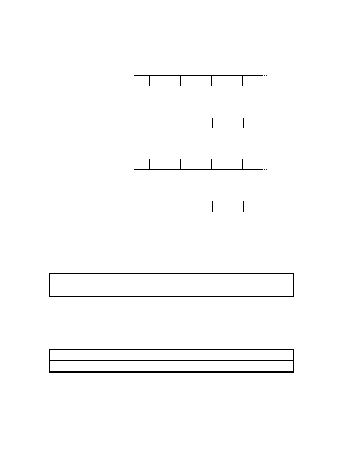
ASYNC FIXE (BIRE) RDYEG RDY RDYI RW16 LPM
⇐ Bit no.
Read/write ⇒
(R/W) (R/W) (R/W) (R) (R) (R/W) (R/W) (R/W)
Default value⇒
(0) (1) (1) (0) (1) (0) (0) (0)
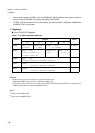
Control Register byte 0
Address : 7000
H
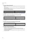
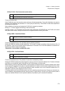
31 30 29 28 27 26 25 24
FMCS
- - - - LOCK PHASE PF2I RD64
⇐ Bit no.
Read/write ⇒
(-) (-) (-) (-) (R/W) (R/W) (R/W) (R/W)
Default value⇒
(X) (X) (X) (X) (0) (0) (0) (0)
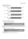
Address : 7001
H
23 22 21 20 19 18 17 16
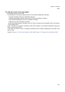
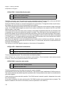
Control Register byte 1
FMCR
- - - - - - REN (TAGE)
⇐ Bit no.
Read/write ⇒
(-) (-) (-) (-) (-) (-) (R/W) (R/W)
Default value⇒
(X) (X) (X) (X) (X) (X) (0) (0)
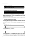
Control Register byte 2
Address : 7002
H
15 14 13 12 11 10 9 8
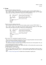
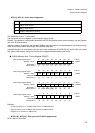
FCHCR
FLUSH (DBEN) PFEN PFMC LOCK ENAB SIZE1 SIZE0
⇐ Bit no.
Read/write ⇒
(R/W) (R
/W
)(R
/W
)(R
/W
) (R/W) (R/W) (R/W) (R/W)
Default value⇒
(1) (0) (0) (0) (0) (0) (1) (1)
Address : 7003
H
765432 10
FCHCR
Control Register byte 3