


760
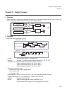
Chapter 37 Output Compare
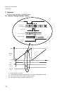
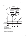
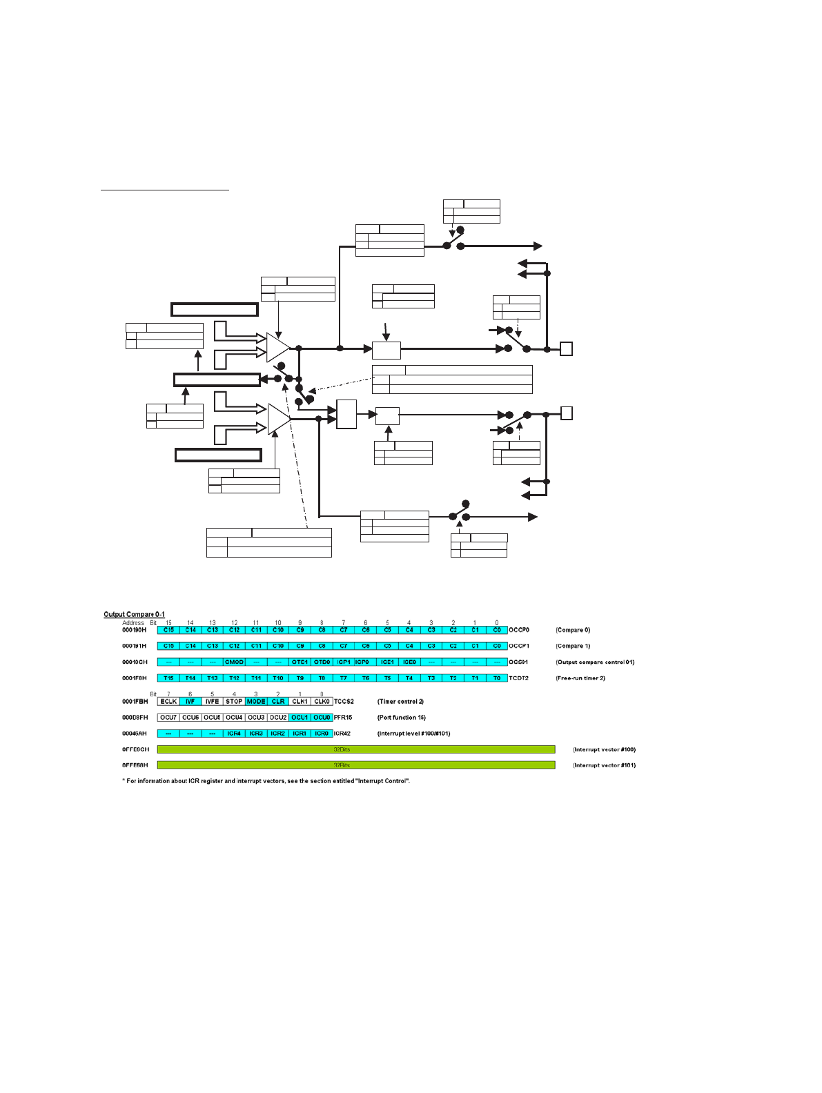
3.Configuration Diagram
3. Configuration Diagram
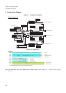
Figure 3-1 Configuration Diagram
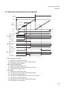
Figure 3-2 Register List
Note: For information about ICR registers and interrupt vectors, see “Chapter 24 Interrupt Control (Page
No.311)”.
Output Compare 0-1
TCDT2
OCCP0
OCU0 Interrupt (#100)
OCU0/TOT0/P15.0
From general-use
port register
General-use port read
Com-
pare
0
Match -> Latch reversal
OCCP1
OCU1 Interrupt (#100)
OCU1/TOT1/P15.1
Com-
pare
1
CST0 OCS01: bit0
0
1
Disable compare operation
Enable compare operation
OT D0
OCS01: bit8
0
1
Low fixed
High fixed
* Compare operation only
writable when stopped
ICE0
OCS01: bit4
0
1
Disable interrupts
Enable interrupts
PFR15.0
0
1
General-use Port
General-use Port
OUT0
PFR15.1
0
1 OUT1
OT D1 OCS01: bit9
0
1
Low fixed 1c
High fixed
* Compare operation only
writable when stopped
CST1 OCS01: bit1
0
1
Disable compare operation
Enable compare operation
ICE1
OCS01: bit5
0
1
Disable interrupts
Enable interrupts
CMOD OCS01: bit12
0 OCCP1 match alone inverts OP1 latch.
External clock (for free-run timer 2)
1
0
0
1
0
OR
MODE
TCCS0 : bit 3
0
1
No clear on compare-match
Clear on compare-match
External clock (for free-run timer 2)
0
1
CLR TCCS2:bit2
0
1
No effect
Clear
IVF
TCCS2: bit6
0
Overflow not present
1
ICP0
OCS01: bit6
0
1
Interrupt request not present
Interrupt request not present
Interrupt request present
Interrupt request present
Write 0: Flag clear
ICP1
OCS01: bit7
0
1
Write 0: Flag clear
1 OCCP0 or OCCP1 match inverts OP1 latch.
0
1
General-use port read
Free-run timer 2
Compare register 0
Compare register 0
From general-use
port register
Latch
Latch
0
0
0
0
0
0
1
0
0
0
0
0
1
Overflow present
0
0
Match -> Latch
reversal