


516
Chapter 31 External Bus
2.External Bus Interface Registers
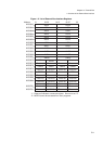
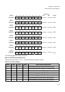
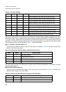
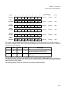
ASZ3-0 are used to set the size of each area by modifying the number of bits for address comparison to a value
different from ASR. Thus, an ASR contains bits that are not compared. Bits ASZ3-0 of ACR0 are initialized to
1111
B
(0F
H
) by RST. Despite this setting, however, the CS0 area just after RST is executed is specially set from
00000000
H
to FFFFFFFF
H
(setting of entire area). The entire-area setting is reset after the first write to ACR0
and an appropriate size is set as indicated in Table 2-1 "Area Size Settings".
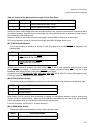
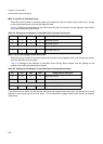
[Bits 11-10] DBW1-0 (Data Bus Width 1-0)
These bits set the data bus width of each chip select area as indicated in Table 2-2 "Setting of the Data Bus
Width of Each Chip Select Area":
The same values as those of the WTH bits of the mode vector are written automatically to bits DBW1-0 of ACR0
during the reset sequence.
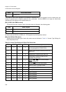
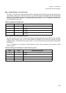
[Bits 9-8] BST1-0 (Burst Size 1-0)
These bits set the maximum burst length of each chip select area as indicated in Table 2-3 "Setting of the
Maximum Burst Length of Each Chip Select".
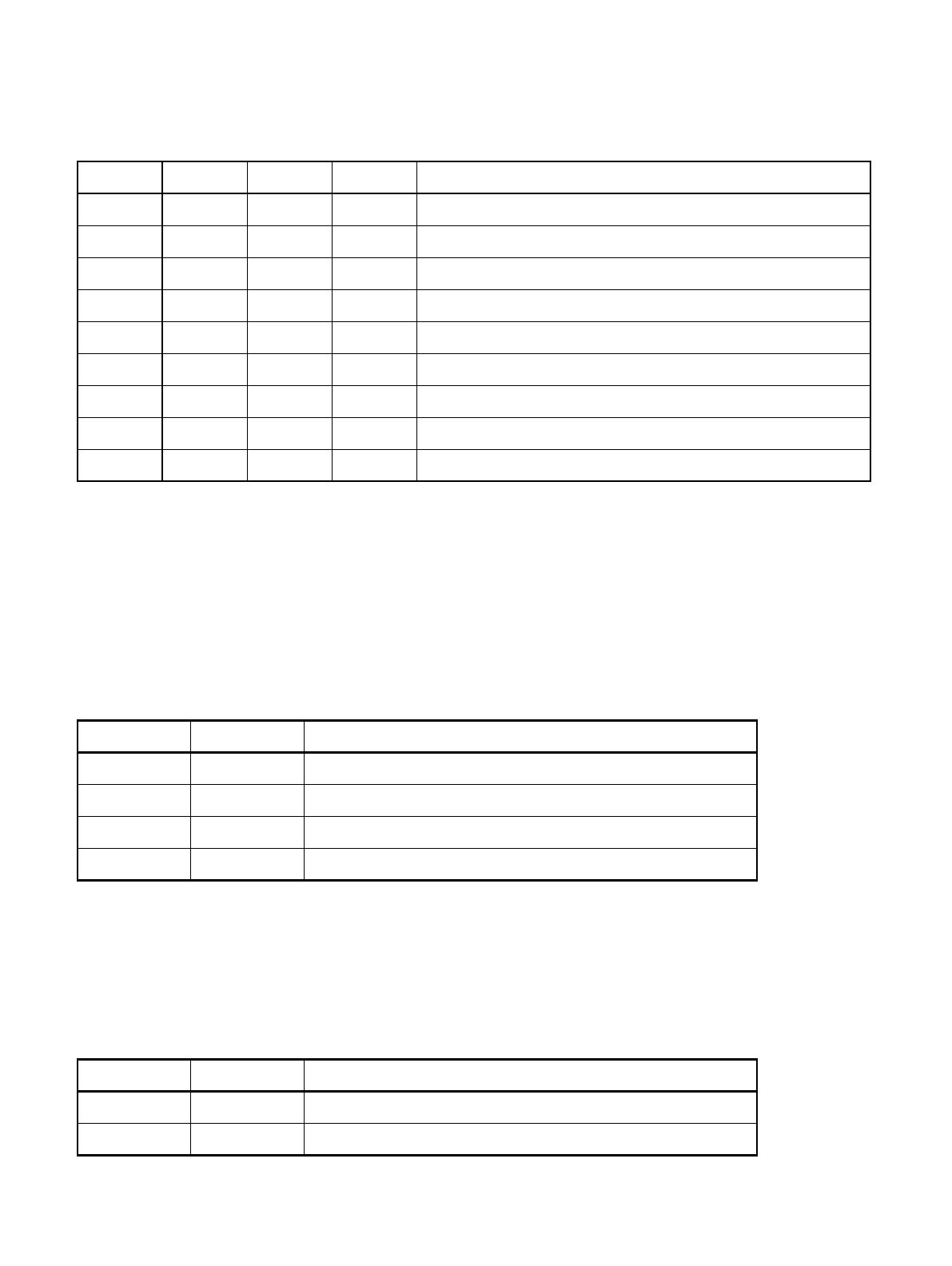
0 1 1 1 8 MB (00800000
H
byte, ASR A[31:23] bits are valid)
1 0 0 0 16 MB (01000000
H
byte, ASR A[31:24] bits are valid)
1 0 0 1 32 MB (02000000
H
byte, ASR A[31:25] bits are valid)
1 0 1 0 64 MB (04000000
H
byte, ASR A[31:26] bits are valid)
1 0 1 1 128 MB (08000000
H
byte, ASR A[31:27] bits are valid)
1 1 0 0 256 MB (10000000
H
byte, ASR A[31:28] bits are valid)
1 1 0 1 512 MB (20000000
H
byte, ASR A[31:29] bits are valid)
1 1 1 0 1024 MB (40000000
H
byte, ASR A[31:30] bits are valid)
1 1 1 1 2048 MB (80000000
H
byte, ASR A[31] bit is valid)
Table 2-2 Setting of the Data Bus Width of Each Chip Select Area
DBW1 DBW0 Data bus width
0 0 8 bits (byte access)
0 1 16 bits (halfword access)
1 0 32 bits (word access)
1 1 Reserved Setting disabled
Table 2-3 Setting of the Maximum Burst Length of Each Chip Select
BST1 BST0 Maximum burst length
0 0 1 (single access)
0 1 2 bursts (address boundary: 1 bit)
Table 2-1 Area Size Settings
ASZ3 ASZ2 ASZ1 ASZ0 Size of each chip select area