


761
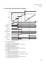
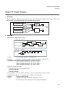
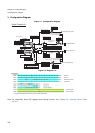
Chapter 37 Output Compare
4.Registers
4. Registers
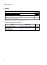
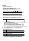
4.1 OCS: Output Control Register
A register for controlling the operation of output compare.
• OCS01 (Output compare 0-1): Address 018Ch (Access: Byte, Half-word, Word)
• OCS23 (Output compare 2-3): Address 018Eh (Access: Byte, Half-word, Word)
• OCS45 (Output compare 4-5): Address 02DCh (Access: Byte, Half-word, Word)
• OCS67 (Output compare 6-7): Address 02DEh (Access: Byte, Half-word, Word)
(For information on attributes, see “Meaning of Bit Attribute Symbols (Page No.10)”.)
• bit15-bit13: undefined Writing does not affect the operation. The read out value is “1”.
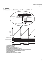
• bit12: Reverse Mode
• Specifies the output level reversal operation of pin OCU1 when free-run timer count value TCDT0
matches compare registers OCCP0, OCCP1.
• When the reverse mode bit is set to “1”, the operation is as follows.
OCU0 pin: output reverses when free-run timer TCDT2 matches compare register 0 (OCCP0)
OCU1 pin: output reverses when free-run timer TCDT2 matches compare register 1 (OCCP1)
• When the reverse mode bit is set to “0”, the operation is as follows.
OCU0 pin: output reverses when free-run timer TCDT2 matches compare register 0(OCCP0)
OCU1 pin: output reverses when free-run timer TCDT2 matches compare register 0 (OCCP0) or
compare register 1 (OCCP1)
Note: Reversal mode does not allow interrupts, even with cooperative operation (CMOD=“1”).
• For output from pins OCU0, OCU1, registers PFR15.0, PFR15.1 must be set.
• bit11-bit10: Undefined Writing does not affect the operation. The read value is “1”.
• bit9: Pin-level settings (output compare 1)
To perform output on pin OCU1, general-purpose port settings must be performed.
• bit8: Pin-level settings (output compare 0)
• To perform output on pin OCU0, general-purpose port settings must be performed.
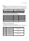
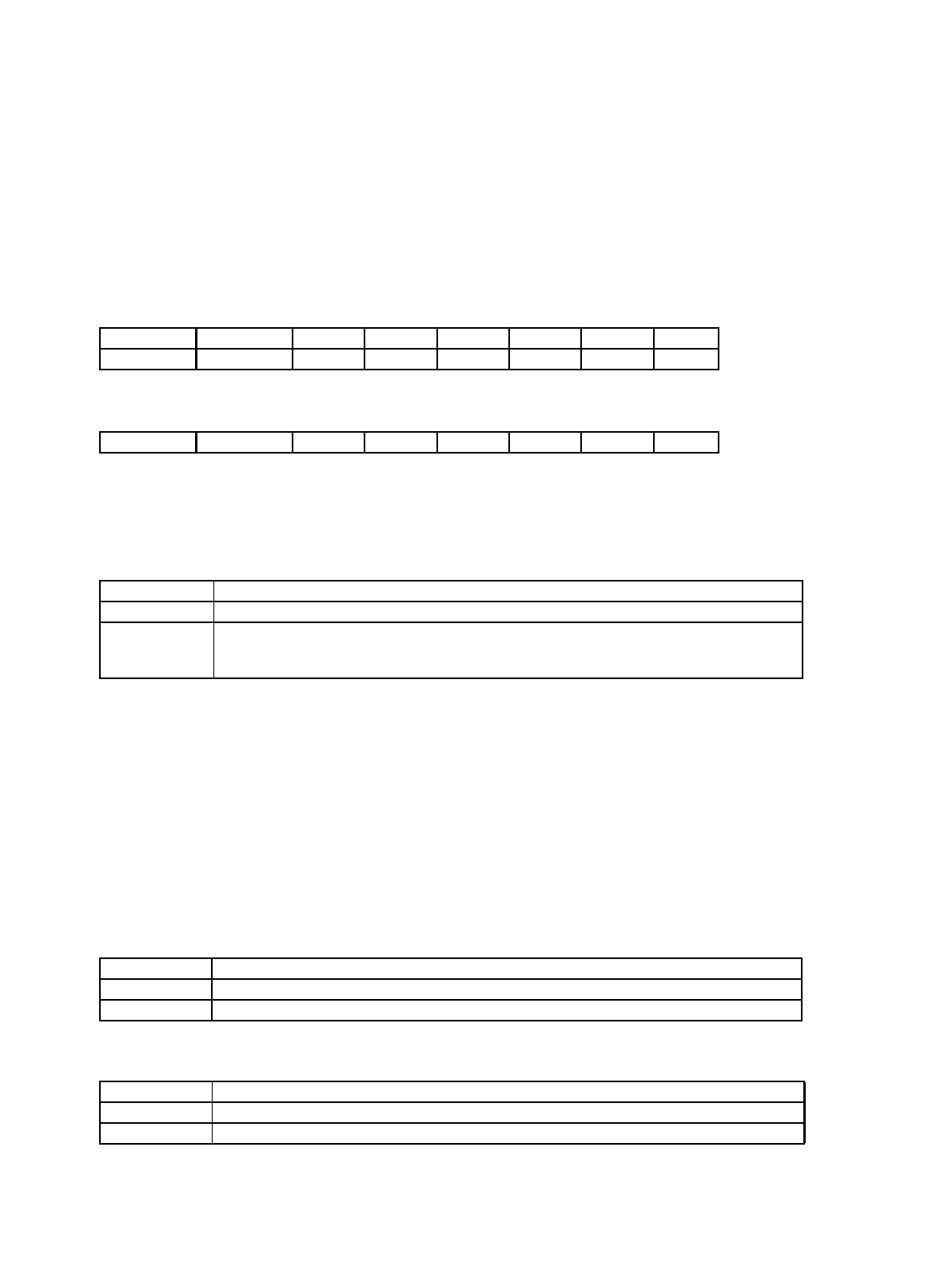
15 14 13 12 11 10 9 8 bit
– – – CMOD – – OTD1 OTD0
1 1 1 0 1 1 0 0 Initial Value
R1/W1 R1/W1 R1/W1 R/W R1/W1 R1/W1 R/W R/W Attribute
7 6 543210bit
ICP1 ICP0 ICE1 ICE0 – – CST1 CST0
0 0 0 0 1 1 0 0 Initial Value
R(RM1),W R(RM1),W R/W R/W R1/W1 R1/W1 R/W R/W Attribute
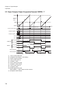
CMOD Operation Mode
0 Independent operation (the output level reversal operation of pins OCU0-OCU1 is independent)
1
Combined operation
(OCU1 output pin level is inverted when output compare 0 or output compare 1 is matched in the
compare operation.)
OTD1 Operation
0 Set the output level of pin OCU1 to “L”
1 Set the output level of pin OCU1 to “H”
OTD0 Operation
0 Set the output level of pin OCU0 to “L”
1 Set the output level of pin OCU0 to “H”