


172
Chapter 11 Memory Controller
8.Explanations of Registers
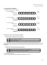
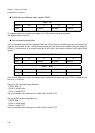
• BIT[17]: PF2I - Prefetch 32 bit (2 instructions) only
When switching on 64 bit read mode (RD64=1) then prefetch will be performed on instruction address
IA+8 (when current access is aligned at IA+0) and on instruction address IA+4 (when current access is
aligned at IA+4). However, the setting of PF2I=1 in the 64 bit read mode will cause a prefetch only on
next instruction address IA+4 (independent of current access alignment is IA+0 or IA+4).
Usually prefetching 64 bit is superior to 32 bit only, however it can be the case on strong fragmented
code that the performance deteriorates due to replacement of cache entries. In this case it can be sen-
sible to switch to 32 bit prefetch only.
• BIT[16]: RD64 - Enable 64 bit read mode
Some embedded FLASH memories supports switching the 64 bit read mode to increase the access per-
formance. Please contact Fujitsu if this feature is available on the product you are using.
This bit is cleared after reset. The 32 bit read and write access to the FLASH memory is enabled by de-
fault.
Setting of the RD64 bit implies switching from 32 bit into 64 bit mode. Writing data to the flash memory
is not supported in the 64 bit read only mode.
Important remark: It is not allowed to switch between the 16 bit, the 32 bit and the 64 bit mode while
reading instructions or data from the FLASH memory.
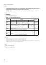
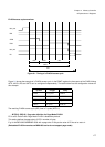
FLASH Cache Control Register (FCHCR)
• BIT[9]: REN - Non-cacheable area Range Enable
The bit is cleared after reset. The address defined in FCHA0 is combined with a bit mask defined in
FCHA1 to define the non-cacheable area.
If the REN bit is set, the non-cacheable area is defined by two points. The non-cacheable range is from
addresses greather than or equal to FCHA0 up to addresses less than or equal to FCHA1.
• BIT[8]: TAGE - TAG RAM access Enable
The bit is set to 0 after reset.
(TAG RAM access is not available on MB91460 series).
0 Prefetch 64 bit (default)
1 Prefetch 32 bit only
0 64 bit read mode is disabled (default)
1 64 bit read mode is enabled
0 FCHA1 defines address mask (default)
1 FCHA1 defines second point for the non-cacheable address range from FCHA0 to FCHA1
0 Memory mapped TAG RAM access disabled (default)
1 Memory mapped TAG RAM access enabled