


937
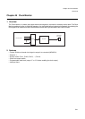
Chapter 47 LCD Controller
7.Q&A
7.2 How do I set VRM?
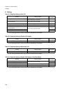
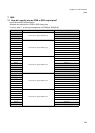
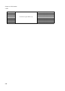
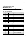
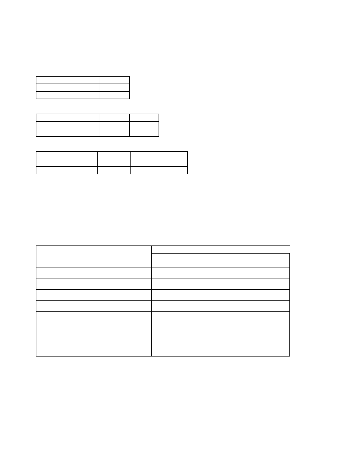
The following tables show the relationship between pins and the bit positions of VRAM(n). (n=0 to 19)
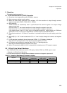
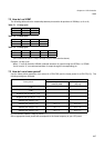
Table 7-1 1/2 duty cycle
Table 7-2 1/3 duty cycle
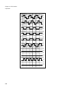
Table 7-3 1/4 duty cycle
(Non-selected waveform is output through the pins other than the above.)
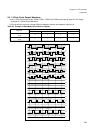
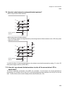
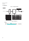
Example: 1/4 duty cycle
When “1” is set to the bit6 of VRAMn, selected waveform is output through the SEG2n+1 of COM2.
If a bit is set to “0”, non-selected waveform is output through the corresponding pin.
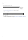
7.3 How do I set a frame period?
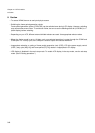
Use the frame period generation clock select bit (LCR0.CSS) and the frame period bit (LCR0.FP[1:0]). The
following settings are available:
N (Time division number) = MS[1:0] value + “1”
Set an appropriate frame period that corresponds to the frame frequency of your LCD panel.
Pin COM1 COM0
SEG 2n bit 1 bit 0
SEG 2n+1 Bit 5 Bit 4
pin COM2 COM1 COM0
SEG 2n bit 2 bit 1 bit 0
SEG 2n+1 Bit 6 Bit 5 Bit 4
pin COM3 COM2 COM1 COM0
SEG 2n bit 3 bit 2 bit 1 bit 0
SEG 2n+1 bit 7 Bit 6 Bit 5 Bit 4
Frame period
Selected value
Frame period generation clock
select bit (CSS)
Frame period bit
(FP[1:0])
Peripheral clock (F
CLKP
)/(2
13
× N)
Set to “0”. Set to “00”.
Peripheral clock (F
CLKP
)/(2
14
× N)
Set to “0”. Set to “01”.
Peripheral clock (F
CLKP
)/(2
15
× N)
Set to “0”. Set to “10”.
Peripheral clock (F
CLKP
)/(2
16
× N)
Set to “0”. Set to “11”.
Subclock (F
CL-SUB
)/(2
3
× N)
Set to “1”. Set to “00”.
Subclock (F
CL-SUB
)/(2
4
× N)
Set to “1”. Set to “01”.
Subclock (F
CL-SUB
)/(2
5
× N)
Set to “1”. Set to “10”.
Subclock (F
CL-SUB
)/(2
6
× N)
Set to “1”. Set to “11”.