


586
Chapter 31 External Bus
9.SDRAM/FCRAM Interface Operation
9.3 Connecting SDRAM/FCRAM to Many Areas
This section shows the connecting SDRAM/FCRAM to many areas.
■ Connecting SDRAM/FCRAM to Many Areas
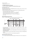
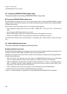
SDRAM/FCRAM can basically be set for all chip select areas. When connecting SDRAM/FCRAM to several
areas, connect the same type of modules. Also it needs considerations about bus load when connecting SDRAM/
FCRAM to several areas.
More precisely, connect the modules common in the following register settings.
• Area configuration register (ACR): Set all of the DBW1 - DBW0, BST1 - BST0, and TYP3 - TYP0 bits to the
same.
• Area wait register (AWR): Set all the bits to the same.
• Memory setting register (MCR): All the settings are the same as the registers are common.)
• Refresh control register (RCR): All the settings are the same as the registers are common.)
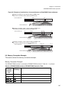
To enable the two areas at a time, execute the power - on sequence, auto - refresh, and self - refresh at the same
time.
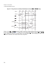
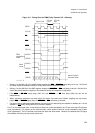
9.4 Address Multiplexing Format
This section describes the address multiplexing format.
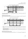
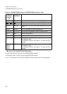
■ Address Multiplexing Format
SDRAM/FCRAM access addresses correspond to row, bank, and column addresses differently depending on the
settings of the ASZ3 to ASZ0, DBW1 and DBW0, PSZ2 to PSZ0, and BANK bits.
Addresses are arranged in the order of Column, BANK, and Row addresses, starting from the least significant bit.
Set each bit as shown below.
• ASZ3 to ASZ0 bits: Set these bits to the total amount of SDRAM/FCRAM connected to the corresponding
area. For using two modules in parallel, set the total amount. Affects the number of row addresses.
• DBW1 and DBW0 bits: Set these bits to the data bus width. (Set the bits to " 16 bits " for connecting a pair of
eight - bit modules in parallel.) Column addresses are shifted according to the data bus width setting. 8 bits:
Do not shift. 16 bits: Shift one bit. 32 bits: Shift two bits.
• PSZ2 to PSZ0 bits: Set these bits to the number of column addresses used for SDRAM/FCRAM.
• BANK bit: Set this bit to the number of SDRAM/FCRAM bank addresses.
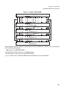
Figure 4.9 - 6 shows examples of combinations of access addresses and Row/BANK/Column addresses.