


911
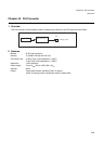
Chapter 45 D/A Converter
4.Registers
4. Registers
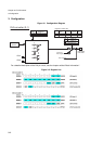
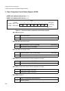
4.1 DADR: D/A Data Register
The D/A Data Register sets the output voltage of the D/A converter.
• DADR0(ch0): Address 0364
H
(Access: Byte, Half-word)
• DADR1(ch1): Address 0366
H
(Access: Byte, Half-word)
(For the attributes, refer to the “Meaning of Bit Attribute Symbols (Page No.10)”.)
• The D/A Data Register is not initialized on a reset.
• The setting is “000
H
” - “3FF
H
”.
4.2 DACR: D/A Control Register
The D/A Control Register controls whether D/A converter output is enabled or disabled.
• DACR(ch0/ch1): Address 0361
H
(Access: Byte)
(For the attributes, refer to the “Meaning of Bit Attribute Symbols (Page No.10)”.)
• bit7-3: Undefined
At write, always write “0”. At read, the read value is indeterminate.
• bit0: D/A output control
• Enables a converted analog level to be output from the DA pin.
(To place the DA0 pin in the output state, it is necessary to set PFR28.6=“1”.
• The D/A output equals 0.0 V when the D/A output control bit is “0”.
• bit1: D/A output control
• Enables a converted analog level to be output from the DA pin.
(To place the DA1 pin in the output state, it is necessary to set PFR28.7=“1”.
• The D/A output equals 0.0 V when the D/A output control bit is “0”.
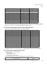
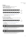
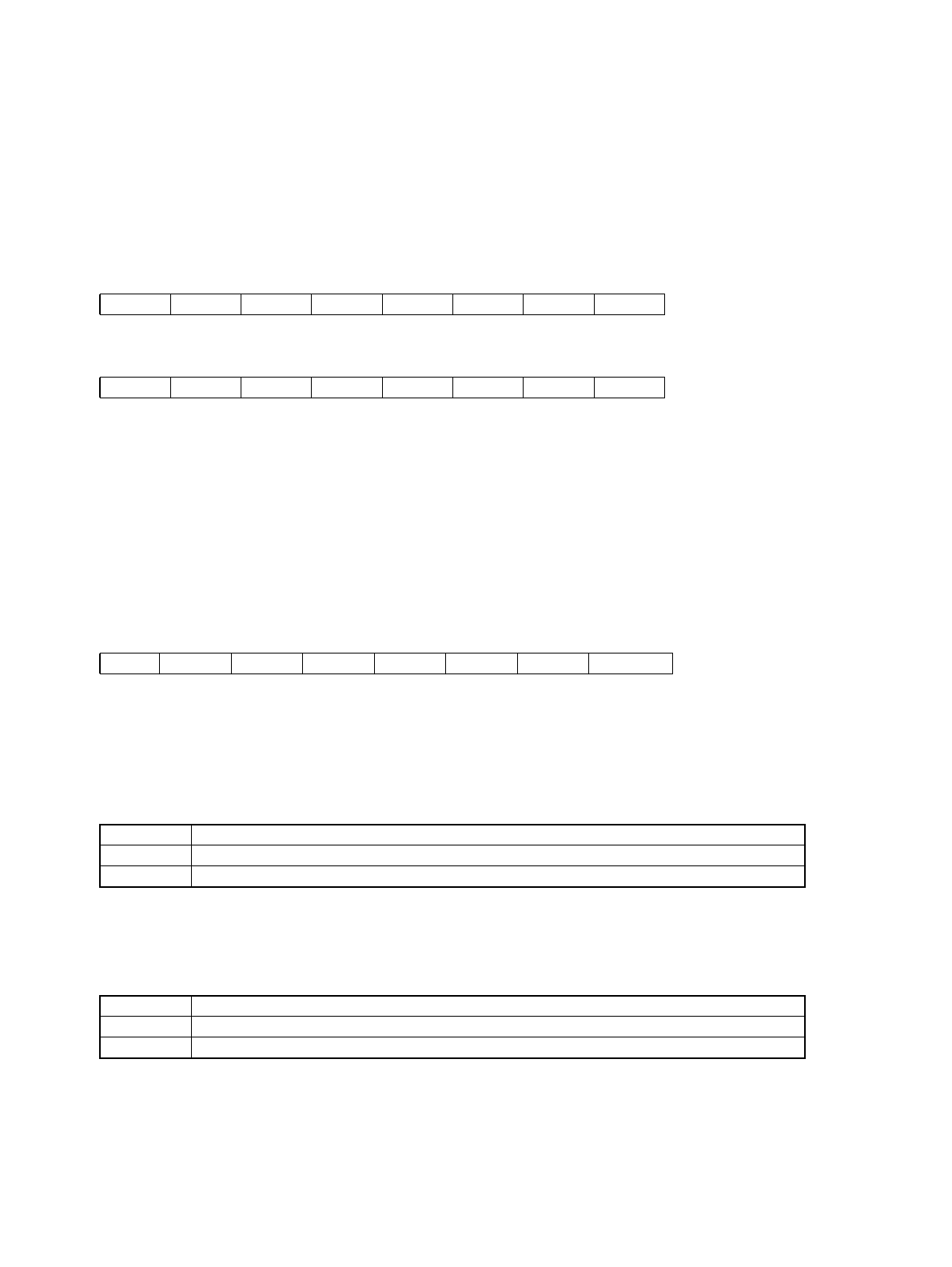
15 14 13 12 11 10 9 8 Bit
------DA9DA8
- - - - - - X X Initial value
RX/W0 RX/W0 RX/W0 RX/W0 RX/W0 RX/W0 R/W R/W Attributes
76543210 Bit
DA7 DA6 DA5 DA4 DA3 DA2 DA1 DA0
XXXXXXXX Initial value
R/W R/W R/W R/W R/W R/W R/W R/W Attributes
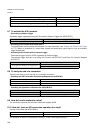
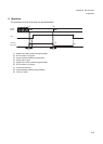
7654321 0 bit
–––––MD08 DAE1 DAE0
–––––00 0 Initial value
RX, W0 RX, W0 RX, W0 RX, W0 RX, W0 R/W R/W R/W Attributes
DAE0 Operation
0 D/A output disabled
1 D/A output enabled
DAE1 Operation
0 D/A output disabled
1 D/A output enabled