


919
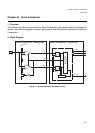
Chapter 46 Alarm Comparator
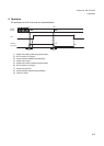
4.Operation Modes
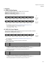
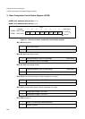
Bit 1: IEN Interrupt enable bit.
Bit 0: PD Power down bit.
4. Operation Modes
The alarm comparator circuit can operate in interrupt or polling mode. The internal interrupt logic will
detect each interrupt event independent from setting of the IEN bit.
4.1 Interrupt Mode (IEN=1)
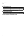
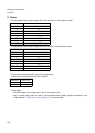
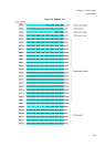
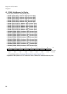
The following truth table describes the valid interrupt events
The interrupt Bit IRQ will be set with the next positive transition of CLKP after detecting an interrupt event.
If IEN=1 this will create an interrupt request to the CPU. In order to determine the reason for the asserted
interrupt - if both interrupts are enabled - it is necessary to read the ACSR register immediately inside the
interrupt service routine. OUT2 and OUT1 always contain the actual status of the comparator outputs, i.e.
the interrupt trigger event will not be stored.
4.2 Polling Mode (IEN=0)
The IRQ register bit will be set by an active interrupt event and can be reset by writing to the ACSR
register.The ACSR can be polled continuously in order to monitor the input voltage which is feed to the AC
comparator inputs.
4.3 Setting and Resetting of IRQ-Flagbit
The IRQ bit of the ACSR register can be reset to zero by writing a “0” to it. Writing an “1” to the IRQ bit of
ACSR register has no effect. IRQ can only be set to “1” by hardware, i.e. by the outputs of the comparator
circuits. IRQ will remain active as long as an active interrupt status is detected, even if a “0” is written to it.
A bitset command performed on the ACSR register will result in a RMW access on the R-Bus. Every read
access during performing a RMW command will return a “1” for the IRQ flag to the CPU. That avoids any
loss in detecting interrupt events due to software setting of IRQ-Flag Bit.
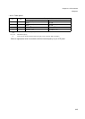
1 Interrupt assertion enabled
0 Interrupt assertion disabled [Initial value]
1 Power down (analog part)
0 Runmode (analog part) [Initial value]
Table 4-1 Valid interrupt events
OUT2 OUT1 IRQ analog input voltage range
1 1 1 Vin > 0.8 AVDD (overvoltage)
1 0 0 0.4 AVDD < Vin < 0.8 AVDD
(normal operation)
0 0 1 Vin < 0.4 AVDD (undervoltage)