


1001
Chapter 54 Flash Memory
7.Auto Algorithms
■ Chip erase
Chip erase (erase all sectors at once) is performed via six accesses. First, there are two “unlock” cycles, after
which a setup command is written. This is then followed by two more “unlock” commands before the chip
erase command.
The user does not have to write to Flash memory before a chip erase can be performed. While the auto erase
algorithm is executing, Flash memory automatically validates each cell before erasing it by writing a “0” pattern
(preprogram). During this operation, the Flash memory does not require external control.
Auto erase begins with a write during the command sequence, and ends when “1” is written to bit 7, at which
point the Flash memory returns to read mode. The time for chip erase is equal to [sector erase time] x [number
of sectors] + [chip write time (preprogram)].
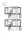
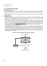
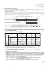
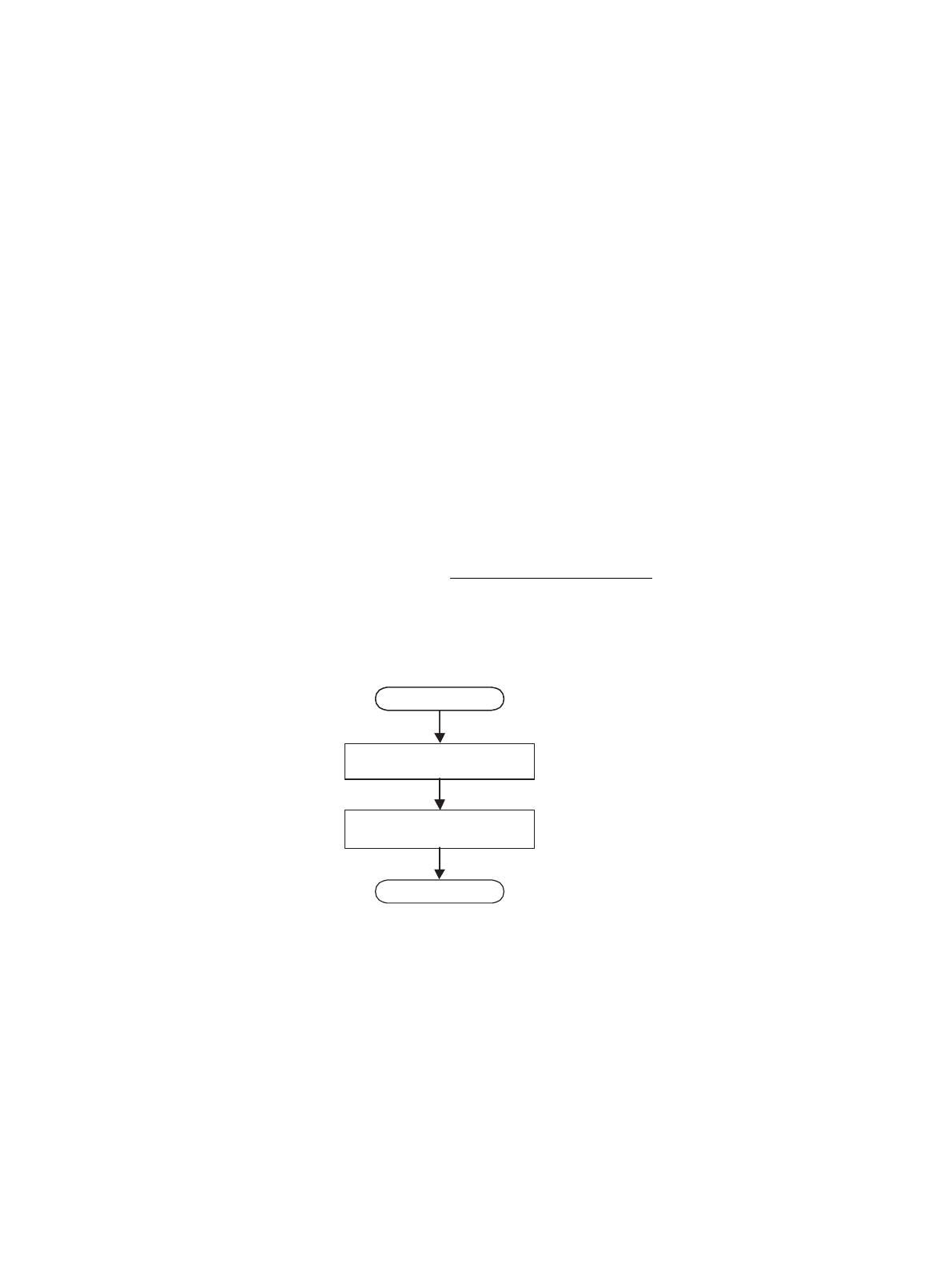
The figure below shows the chip erase sequence using the chip erase command.
■ Sector erase
Sector erase is performed via six accesses. There are two “unlock” cycles, after which a “setup” command is
written, followed by another two “unlock” cycles. On the sixth cycle, a sector erase command is input, starting
the sector erase. From the time that the last sector-erase command is written until the timeout of 50us, the
next sector-erase command will be accepted.
It is possible to submit multiple sector erases simultaneously by writing the six bus cycles described above.
This sequence is performed by writing the addresses of sectors to erase in succession after the sector-erase
command (30
H
). After a timeout of 50us since the last sector-erase command was written, sector erase
begins. In other words, to erase multiple sectors simultaneously, each sector must be entered within 50us of
the other, after which commands may no longer be accepted. It is possible to monitor whether successive
sector-erase commands are valid via bit 3 (see (3) Hardware sequence flag). After finishing, Flash memory
returns to read mode. Other commands are ignored. Data polling works on any address in an erased sector.
The time for multiple-sector erase is equal to ([sector erase time] + [sector write time (preprogram)]) x [number
of sectors erased].
Figure 7-2 Chip Erase Sequence Using the Chip erase Command
■ Erase suspend
The erase suspend command allows the user to pause the Flash memory’s Auto Algorithm during sector
erase, and read data from/write data to sectors not being erased. This command is only valid during sector
erase. It is ignored during chip erase and write operations. The erase suspend command (B0
H
) is only valid
during sector-erase operation, including the timeout period after a sector-erase command (30
H
). Entering this
command during the timeout period immediately ends the timeout, and interrupts the erase operation. When
the erase resume command is written, the erase operation resumes. Any address can be used for erase
suspend and erase resume command input.
If a erase suspend command is input during sector-erase operation, it will take up to 20us for the Flash
memory to halt the erase operation. When the Flash memory goes into erase suspend mode, it outputs ready/
busy and bit 7 outputs “1”, and bit-6 toggling is halted. It is possible to confirm whether the erase operation
/
Start erase
Chip/sector erase
command sequence
Device data polling or
toggle bit complete
Write finished