682
Chapter 33 I2C Controller
2.I2C Interface Registers
2.8 Clock Control Register (ICCR0)
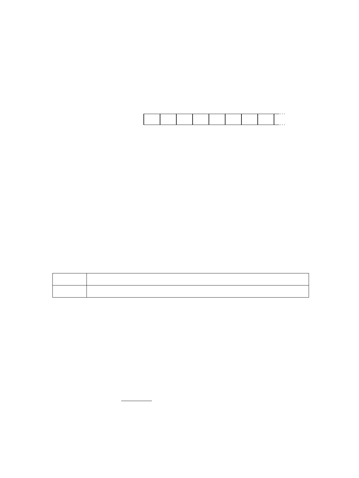
The clock control register (ICCR0) has the following functions:
• Enable IO pad noise filters
• Enable I
2
C interface operation
• Setting the serial clock frequency
[bit 15] Not used.
This bit always reads ‘0’.
[bit 14] IO pad NoiSe Filter enable.
This bit enables the noise filters built into the SDA and SCL IO pads.
The noise filter will suppress single spikes with a pulse width of 0 ns (minimum) and between 1 and 1.5 cycles
of R-bus (maximum). The maximum depends on the phase relationship between I
2
C signals (SDA, SCL) and
R-bus clock.
It should be set to ‘1’ if the interface is transmitting or receiving at datarates above 100 kBit.
[bit 13] EN (ENable)
This bit enables the I
2
C interface operation. It can only be set by the user but may be cleared by the user and
the hardware.
When this bit is set to ‘0’ all bits in the IBSR0 register and IBCR0 register (except the BER and BEIE bits) are
cleared, the module is disabled and the I
2
C lines are left open. It is cleared by the hardware if a bus error
occurs (BER=‘1’ in IBCR0).
Warning: The interface immediately stops transmitting or receiving if is it is being disabled. This might leave
the I
2
C bus in an undesired state!
[bit 12] - [bit 8] CS4-0 (Clock preScaler)
These bits select the serial bitrate. They can only be changed if the interface is disabled (EN=‘0’) or the EN bit
is being cleared in the same write access.
It is determined by the following formula:
0 Interface disabled.
1 Interface enabled.
--- NSF EN CS4 CS3 CS2 CS1 CS0
⇐ Bit no.
Read/write ⇒
(-) (R/W) (R/W) (R/W) (R/W) (R/W) (R/W) (R/W)
Default value⇒
(0) (0) (0) (1) (1) (1) (1) (1)
Clock Control register
Address : 0000DA
H
15 14 13 12 11 10 9 8
ICCR0
Bitrate =
n*12 + 18
φ
n>0; φ : R-Bus clock CLKP (set by DIVR0 register)
Noise filter disabled


