


424
Chapter 29 MPU / EDSU
4.Registers
The COMB bit set to ’1’ causes the IA comparator CMP0 to use the same BADx point definitions as the OA com-
parator CMP1. Point 3 and Point 2 define the address range for both comparators CMP0 and CMP1. This has the
effect that the entry of Point 0/Mask 0 is not allocated for the Point set-up and could be used for masking either one
or both comparators. The Point 1 entry is not useable in this case.
If the COMB bit is set to ’0’ both comparators have independent address configurations. The comparators can either
define read/write permissions for data protection or define execute permissions for code protection. Each compa-
rator can define an address region by a range between two points (ER=1) or by one point with a mask (EM=1).
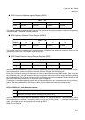
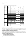
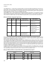
BIT[13:12]: CTC[1:0] - Comparator Type Config
One group of channels contains 2 range comparator blocks. Each comparator block can detect a range hit between
two points or two independent point hits. The point configuration is stored in dedicated BADx registsers for each
channel (4 BADx registers for each group of channels).
The comparator type configuration (CTC) controls the input multiplexing of the compare value for each of the two
range comparator blocks CMP1 and CMP0. CMP1 combines the break detection channels 3 and 2. The compare
value for CMP1 can be assigned either to the instruction address (IA) or to the operand address (OA). CMP0 com-
bines the break detection channels 1 and 0. The compare value for CMP0 can be assigned to the instruction ad-
dress (IA), to the operand address (OA) or to the data value (DT). The table above defines the input compare values
for CMP1 and CMP0, depending on the CTC setting.
In addition a mask for each comparator block could be defined (see the definition of the EM bits later). In this case
the BADx register, which contains the mask information, is not available for the point configuration. Thus the usage
of the mask feature restricts the number of points or channels, which are available in total.
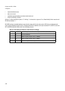
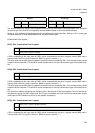
BIT[11:8]: OBS[1:0], OBT[1:0] - Operand Break Size / Operand Break Type register 1
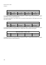
CTC CMP1 CMP0 Break Function MPU Function
0 IA IA 4 instruction break points 2 regions for code protection
(x permissions)
1 OA OA 4 operand break points 2 regions for data protection
(rw permissions)
2 OA IA 2 instruction break points +
2 operand break points
1 region for code protection
(x permissions) and
1 region for data protection
(rw permissions) or
1 region for combined code
and data protection
(rwx permissions)
3 OA DT 2 operand break points +
2 data value breaks,
normally with combination
not applicable
Datasize Access type
OBS1 OBS0 OBT1 OBT0
0 0 Byte (Default) 0 0 Read (Default)
0 1 Halfword 0 1 Read-Modify-Write
1 0 Word 1 0 Write