


571
Chapter 31 External Bus
5.Operation of the Ordinary bus interface
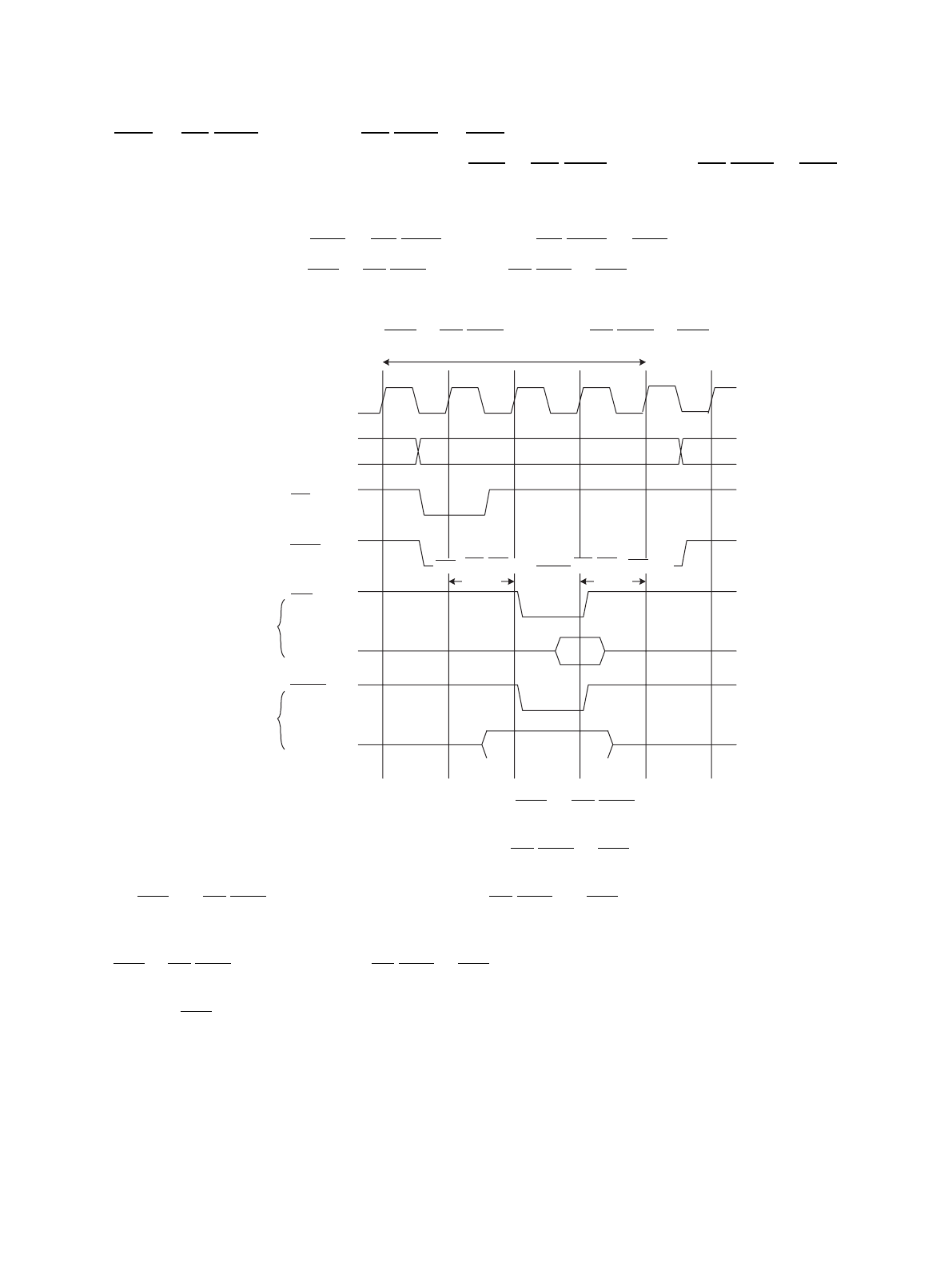
5.9 CSn -> RD/WRn Setup and RD/WRn -> CSn Hold Setting
This section shows the operation timing for the
CSn -> RD/WRn setup and RD/WRn -> CSn hold
settings.
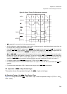
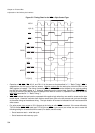
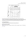
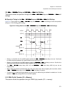
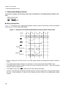
■ Operation Timing for the CSn -> RD/WRn Setup and RD/WRn -> CSn Hold Settings
Figure 5-9 "Timing Chart for the CSn -> RD/WRn Setup and RD/WRn -> CSn Hold Settings" shows the operation
timing for (TYP3-0=0000
B
AWR=000B
H
).
Figure 5-9 Timing Chart for the CSn -> RD/WRn Setup and RD/WRn -> CSn Hold Settings
• Setting 1 for the W01 bit of the AWR register enables the CSn -> RD/WRn setup delay to be set. Set this bit
to extend the period between chip select assertion and read/write strobe.
• Setting 1 for the W00 bit of the AWR register enables the RD/WRn -> CSn hold delay to be set. Set this bit to
extend the period between read/write strobe negation and chip select negation.
• The CSn -> RD/WRn setup delay (W01 bit) and RD/WRn -> CSn hold delay (W00 bit) can be set
independently.
• When making successive accesses within the same chip select area without negating the chip select, neither
a CSn -> RD/WRn setup delay nor an RD/WRn -> CSn hold delay is inserted.
• If a setup cycle for determining the address or a hold cycle for determining the address is needed, set 1 for the
address -> CSn delay setting (W02 bit of the AWR register).
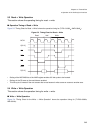
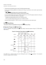
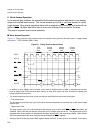
5.10 DMA Fly-By Transfer (I/O -> Memory)
This section shows the operation timing for DMA fly-by transfer (I/O -> memory).
READ
WRITE
MCLK
AS
CSn
RD
D[31:0]
WRn
D[31:0]
A[31:0]
CS->RD/WR
Delay
RD/WR->CS
Delay