


702
Chapter 34 CAN Controller
2.Register Description
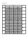
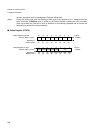
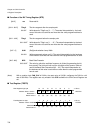
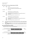
■ Function of the Bit Timing Register (BTR)
(Note) With a module clock CAN_CLK of 8 MHz, the reset value of 0x2301 configures the CAN for a bit
rate of 500 kBit/s. The registers are only writable if bits CCE and Init in the CAN Control Register are
set.
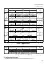
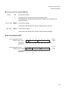
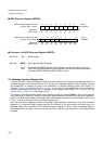
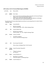
■ Test Register (TESTR)
[bit15] res Reserved bit
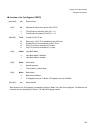
[bit14 - bit12] TSeg2 The time segment after the sample point
0x0-0x7 Valid values for TSeg2 are [ 0 … 7 ]. The actual interpretation by the hard-
ware of this value is such that one more than the value programmed here is
used.
[bit11 - bit8] TSeg1 The time segment before the sample point
0x01-0x0F Valid values for TSeg1 are [ 1 … 15 ]. The actual interpretation by the hard-
ware of this value is such that one more than the value programmed here is
used
[bit7 - 6] SJW (Re)Synchronisation Jump Width
0x0-0x3 Valid programmed values are 0-3. The actual interpretation by the hardware
of this value is such that one more than the value programmed here is used.
[bit5 - bit0] BRP Baud Rate Prescaler
0x00-0x3F The value by which the oscillator frequency is divided for generating the bit
time quanta. The bit time is built up from a multiple of this quanta. Valid val-
ues for the Baud Rate Prescaler are[0 … 63]. The actual interpretation by
the hardware of this value is such that one more than the value programmed
here is used.
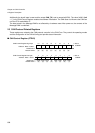
res res res res res res res res
⇐ Bit no.
Read/write ⇒
(R) (R) (R) (R) (R) (R) (R) (R)
Default value⇒
(0) (0) (0) (0) (0) (0) (0) (0)
Test Register high byte
Address : Base + 0x0A
H
15 14 13 12 11 10 9 8
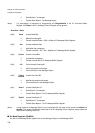
TESTRH
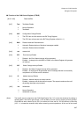
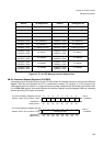
Rx Tx1 Tx0 LBack Silent Basic res res
⇐ Bit no.
Read/write ⇒
(R) (R/W) (R/W) (R/W) (R/W) (R/W) (R) (R)
Default value⇒
(0) (0) (0) (0) (0) (0) (0) (0)
Address :
Base + 0x
0BH
765432 10
TESTRL
Test Register low byte