


529
Chapter 31 External Bus
2.External Bus Interface Registers
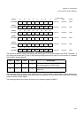
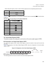
■ Structure of the Memory Setting Register (MCRA for SDRAM/FCRAM auto - precharge OFF
mode)
Memory setting register (MCRA for SDRAM/FCRAM auto - precharge OFF mode)
The memory setting register (MCRA: Memory Setting Register for extend type - A for SDRAM/FCRAM auto -
precharge OFF mode) is used to make various settings for SDRAM/FCRAM connected to the chip select area.
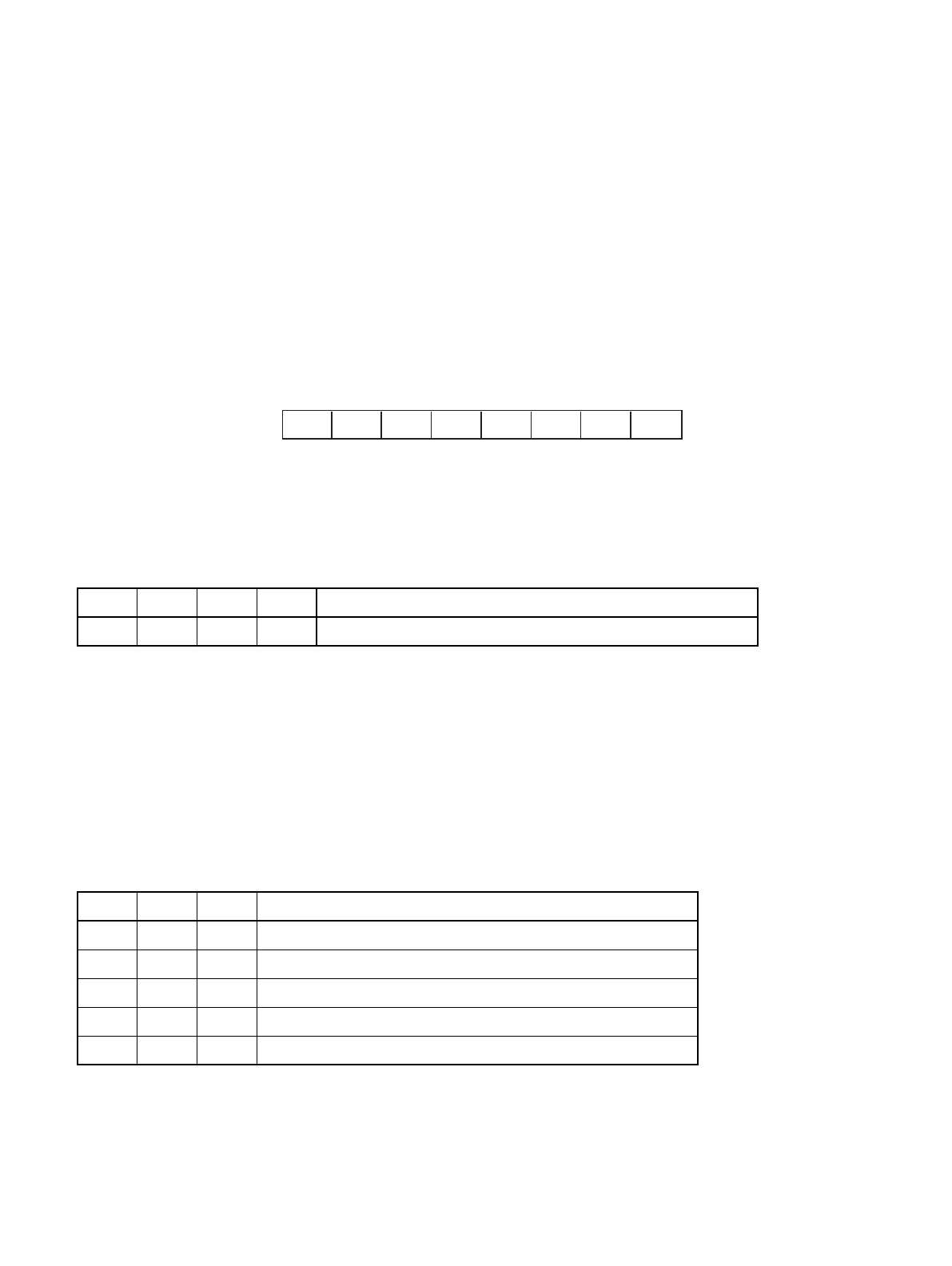
Figure 2-4 shows the bit configuration of the memory setting register (MCRA for SDRAM/FCRAM auto -
precharge OFF mode).
Figure 2-4 Bit configuration of the memory setting register (MCRA for SDRAM/FCRAM auto - precharge
OFF mode)
The register serves as the area for making various settings for SDRAM/FCRAM connected to the chip select area
for which the access type (TYP3 to TYP0 bits) in the ACR6 and ACR7 registers has been set as in Table 2-25 .
Table 2-25 lists the access type settings (TYP3 to TYP0 bits).
MCRB shares register hardware with MCRA. Updating the MCRA therefore updates the MCRB accordingly.
The following summarizes the functions of individual bits in the memory setting register (MCRA for SDRAM/
FCRAM auto - precharge OFF mode).
[Bit 31] Reserved bit
Be sure to set this bit to 0.
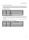
[Bits 30 - 28] PSZ2, PSZ1, PSZ0 (Page SiZe): Page size
Set these bits to the page size of SDRAM to be connected.
Table 2-26 lists the settings for the page size of SDRAM connected.
[Bit 27] WBST (Write BurST enable): Write burst setting
Set this bit to select whether to burst - write for write access.
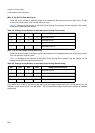
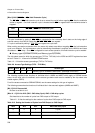
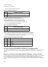
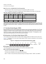
Table 2-16 Access type settings (TYP3 to TYP0 bits)
TYP3 TYP2 TYP1 TYP0 Access type
1000Memory type A:SDRAM/FCRAM(not used auto precharge)
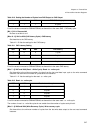
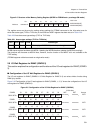
Table 2-17 Settings for the page size of SDRAM
PSZ2 PSZ1 PSZ0 Page size of SDRAM
0 0 0 8-bit column address:A0 to A7(256 memory words)
0 0 1 9-bit column address:A0 to A8(512 memory words)
0 1 0 10-bit column address:A0 to A9(1024 memory words)
0 1 1 11-bit column address:A0 to A9, A11(2048memory words)
1 X X Prohibited
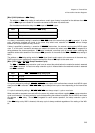
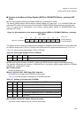
31 30 29 28 27 26 25 24
00000670
H
Reserved PSZ2 PSZ1 PSZ0 WBST BANK ABS1 ABS0
Initial value
Address
bit
XXXXXXXX
B
(INIT)
XXXXXXXX
B
(RST)
R/W R/W R/W R/W R/W R/W R/W R/W