


893
Chapter 44 A/D Converter
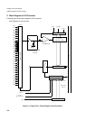
3.Registers of A/D Converter
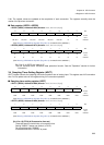
2-bit. The register values are updated at the completion of each conversion. The registers normally store the
results of the previous conversion.
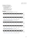
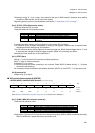
■ Data register (ADCR1, ADCR0)
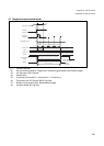
• ADCR1 (ADC0): Address 01A6h (Access: Word, Half-word, Byte)
(See “Meaning of Bit Attribute Symbols (Page No.10)” for details of the attributes.)
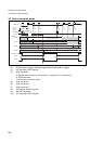
• ADCR0 (ADC0): Address 01A7h (Access: Word, Half-word, Byte)
(See “Meaning of Bit Attribute Symbols (Page No.10)” for details of the attributes.)
Bit 15 to 10 of ADCR1 are read as "0".
The A/D converter has a conversion data protection function. See the "Operation" section for further
information.
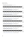
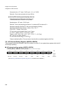
3.4 Sampling Timer Setting Register (ADCT)
ADCT register controls the sampling time and conversion time of analog input. This register sets A/D conversion
time. Do not update value of this register during A/D conversion operation.
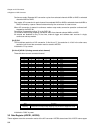
■ Sampling timer setting register (ADCT)
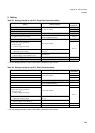
• ADCT1 (ADC0): Address 01A8h (Access: Word, Half-word, Byte)
(See “Meaning of Bit Attribute Symbols (Page No.10)” for details of the attributes.)
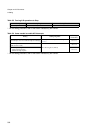
• ADCT0 (ADC0): Address 01A9h (Access: Word, Half-word, Byte)
(See “Meaning of Bit Attribute Symbols (Page No.10)” for details of the attributes.)
[bit 15 to 10] CT5-0 (A/D conversion time set)
These bits specify clock division of conversion time.
Setting "000001" means one division (=CLKP).
Do not set these bits "000000".
Initialized these bits to "000100" by reset.
15 14 13 12 11 10 9 8 Bit
------D9D8
------XX
Initial
value
RX, W0 RX, W0 RX, W0 RX, W0 RX, W0 RX, W0 R R Attribute
76543210Bit
D7 D6 D5 D4 D3 D2 D1 D0
XXXXXXXX
Initial
value
RRRRRRRRAttribute
15 14 13 12 11 10 9 8 Bit
CT5 CT4 CT3 CT2 CT1 CT0 ST9 ST8
00010000
Initial
value
R/W R/W R/W R/W R/W R/W R/W R/W Attribute
76543210Bit
ST7 ST6 ST5 ST4 ST3 ST2 ST1 ST0
00101100
Initial
value
R/W R/W R/W R/W R/W R/W R/W R/W Attribute