


423
Chapter 29 MPU / EDSU
4.Registers
Some restrictions apply with the setting of the MPE bit.
MPE=0 (break unit):
• permission registers are don’t care (BCRx bits [23:16])
MPE=1 (memory protection unit):
• OBS and OBT should be set to ’3’ (BCRx bits [11:8], any size and any type)
• CTC should not be set to ’3’ (BCRx bits [13:12], data value check not supported in this mode)
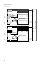
BIT[14]: COMB - Channel Combination Enable
Depending on the MPE configuration bit the COMB feature has different meaning.
(A) COMB=1 and MPE=0 (break unit, combined operand address and data value break):
The break detection conditions are combined before setting the BIRQ_BD bits and signalizing an operand break
condition. Setting the COMB bit is required for defining a data value break on a specific operand address. If the
COMB bit is set to ’1’, both conditions, matching operand address (OA) and matching data value (DT), are required
to be true. Setting the COMB bit makes only sense in the OA/DT mode, defined by CTC=3.
The AND-combination is effective between channels 3 (OA1) and 1 (DT1) and between channels 2 (OA0) and 0
(DT0). It is assumed that no range operation is defined (ER1=ER0=0).
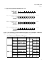
BIRQ_BD3 = BIRQ_BD1 = BD3 && BD1;
BIRQ_BD2 = BIRQ_BD0 = BD2 && BD0;
If channels 3 and 2 define an operand address range (OA1:OA0) by setting ER1=1 and/or channels 1 and 0 define
a data value range (DT1:DT0) by setting ER0=1, the break detection bits of each channel are AND-combined with
the ORed channels of the opposite range comparator break detection outputs.
BIRQ_BD3 = BD3 && (BD1 || BD0);
BIRQ_BD2 = BD2 && (BD1 || BD0);
BIRQ_BD1 = BD1 && (BD3 || BD2);
BIRQ_BD0 = BD0 && (BD3 || BD2);
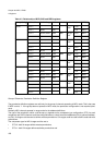
This offers the same interpretation of the BIRQ break detction bits (see table 4-2 for coding of match on start point,
range or end point) as it would be the case for range detection with COMB=0. BD3 and BD2 hold the coding for the
operand address (OA) match, whereas BD1 and BD0 hold the coding for the data value (DT) match. The COMB bit
set to ’1’ ensures that both conditions, the OA match and the DT match must be true to set the appropriate BD bit
in the end.
If the COMB bit is set to ’0’ all break detection bits are passed to the BIRQ register in it’s original form. The compa-
rator channels match conditions are independent from each other.
(B) COMB=1 and MPE=1 (memory protection unit, combined rwx permissions on single range):
In memory protection mode the COMB bit has the meaning of combined data read/write and code execute permis-
sions, set for the same address range. The setting is only meaningful for the combination of operand address (OA)
comparators on channels 3 and 2 and instruction address (IA) comparators on channels 1 and 2 in the mode
CTC=2.
1 The group of channels operates in memory protection mode
0 No combination between channels (default)
1 Combination between channels is effective