


924
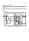
Chapter 47 LCD Controller
4.Registers
4. Registers
4.1 LCR0: LCDC Control Register 0
This register is used to select a frame period and its clock and the display mode, to enable/disable LCD display and
the operation in the watch mode, and to control the drive power source.
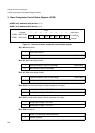
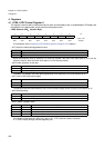
• LCR0: Address 0E9
H
(Access: Byte)
(For attributes, refer to “Meaning of Bit Attribute Symbols (Page No.10)” chapter.)
• bit7: Select the frame period generation clock
When the peripheral clock is selected, LCD does not operate if the main clock stops (that is, LCD is in the
subclock mode in which the main clock stops, or in the sub-stop mode).
• bit6: Enable operation in sub-stop
To enable LCD display, the frame period generation clock select bit (CCS) must be also set to “1”.
• bit5: Control LCD drive power supply
To connect external divided resistors, the LCD drive power supply control bit (VSEL) must be set to “0”.
• bit4: Select blanking
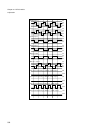
• bit3-2: Select a display mode
If the display mode select bit (MS[1:0]) is set to “00”, LCD Controller ceases to operate.
A “L” level is output through common/segment pins.
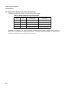
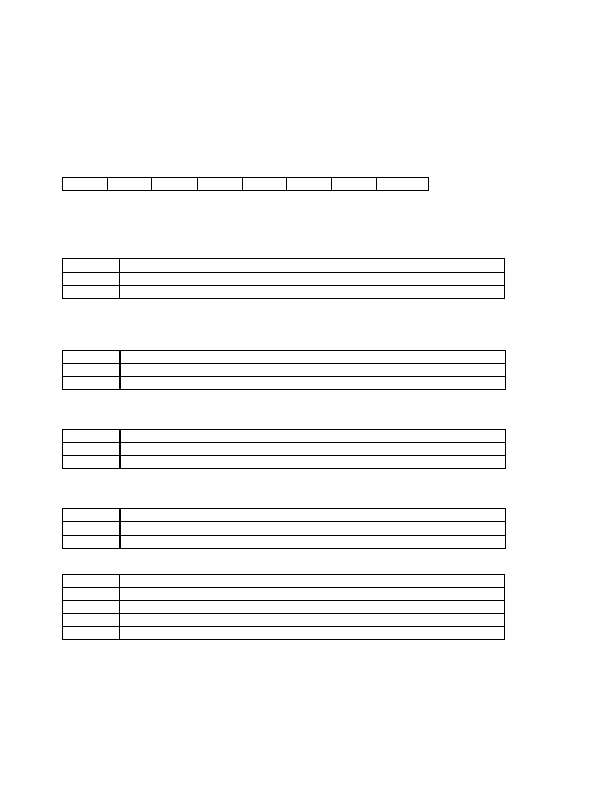
7654321 0 bit
CSS LCEN VSEL BK MS1 MS0 FP1 FP0
0001000 0Initial value
R/W R/W R/W R/W R/W R/W R/W R/W Attribute
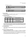
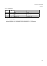
CSS Operation
0 Peripheral clock (CLKP)
1 Subclock
LCEN Operation
0 Disable LCD display in the sub-stop mode.
1 Enable LCD display in the sub-stop mode.
VSEL Operation
0 Disconnect internal divided resistors.
1 Connect internal divided resistors.
BK Operation
0 Enable LCD display.
1 Disable (blank) LCD display.
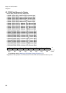
MS1 MS0 Display mode
0 0 Deactivate LCD.
0 1 1/2 duty cycle output mode (Time division number: N=2, COM0-COM1)
1 0 1/3 duty cycle output mode (Time division number: N=3, COM0-COM2)
1 1 1/4 duty cycle output mode (Time division number: N=4, COM0-COM3)