


650
Chapter 32 USART (LIN / FIFO)
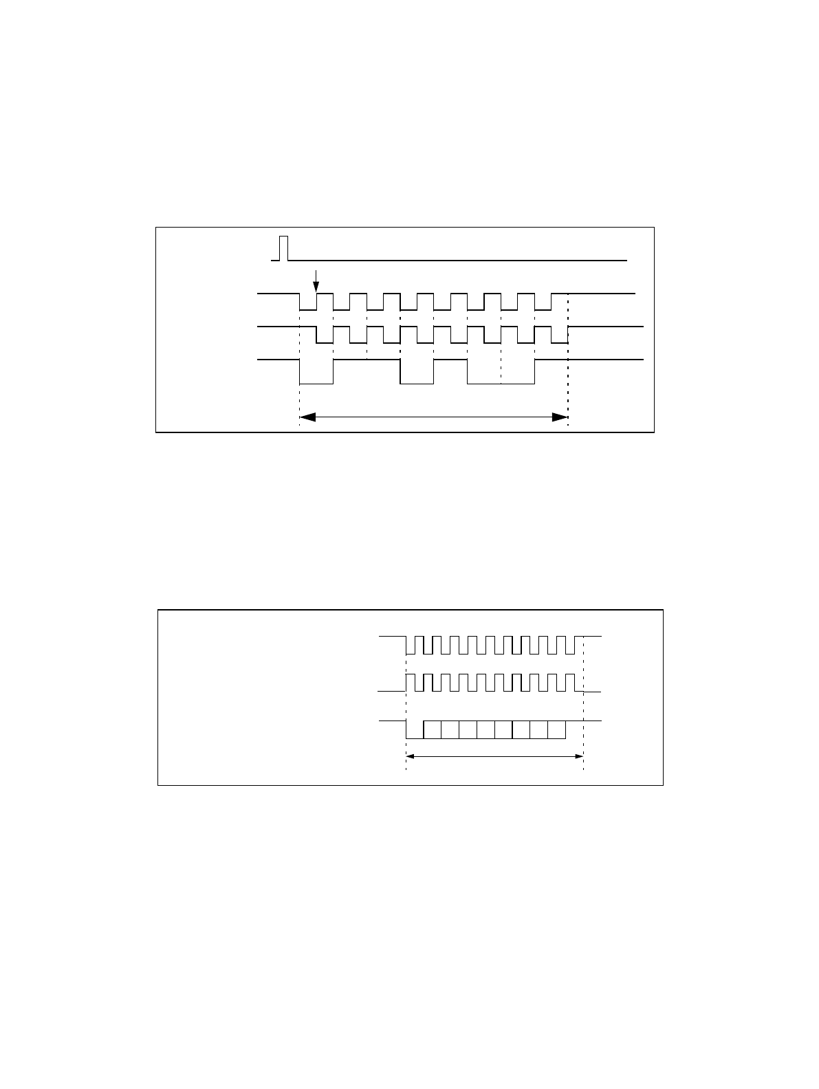
7.USART Operation
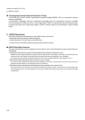
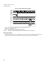
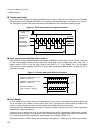
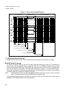
■ Transfer data format
In the synchronous mode, 8-bit data is transferred with no start or stop bits if the SSM bit of the Extended
Communication Control Register (ECCR04) is 0. A special clock signal belongs to the data format in mode 2.
The figure below illustrates the data format during a transmission in the synchronous operation mode.
Figure 7-3 SPI Transfer data format (operation mode 2)
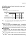
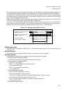
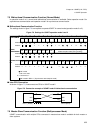
■ Clock inversion and start/stop bits in mode 2
If the SCES bit of the Extended Status/Control Register (ESCR04) is set the serial clock is inverted. Therefore
in slave mode USART samples the data bits at the falling edge of the received serial clock. Note, that in
master mode if SCES is set the clock signal’s mark level is “0”. If the SSM04 bit of the Extended
Communication Control Register (ECCR04) is set the data format gets additional start and stop bits like in
asynchronous mode
Figure 7-4 Transfer data format with clock inversion
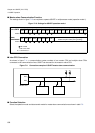
■ Clock Supply
In clock synchronous (normal) mode (I/O extended serial), the number of the transmission and reception bits
has to be equal to the number of clock cycles. Note, that if start/stop bits communication is enabled, the
number of clock cycles has to match with the quantity for the additional start and stop bit(s).
If the internal clock (dedicated reload counter) is selected, the data receiving synchronous clock is generated
automatically if data is transmitted.
If external clock is selected, be sure, that the transmission side of the Transmission Data Register contains
data and then clock cycles for each bit to sent have to be generated and supplied from outside. The mark level
("H") must be retained before transmission starts and after it is complete if SCES is “0”.
Setting the SCDE bit of ECCR delays the transmitting clock signal by 1 CLKP cycle (or half a clock period in
Transmission data
writing
Transmitting or
receiving clock
Transmission and
reception data
0 1 1 0 1 0 0 1
Data
LSB MSB
Mark level
(normal)
Transmitting
clock (SCDE = 1)
Mark level
Mark level
Reception data sample edge (SCES = 0)
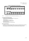
data frame
reception or transmission clock
data stream (SSM = 1)
(here: no parity, 1 stop bit)
ST
SP
(SCES = 0, CCO = 0):
reception or transmission clock
(SCES = 1, CCO = 0):
mark level
mark level