


563
Chapter 31 External Bus
5.Operation of the Ordinary bus interface
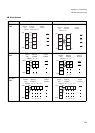
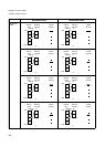
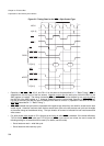
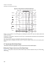
Figure 5-1 Basic Timing (For Successive Accesses)
• AS is asserted for one cycle in the bus access start cycle.
• A31-0 continues to output the address of the location of the start byte in word/halfword/byte access from the
bus access start cycle to the bus access end cycle.
• If the W02 bit of the AWR0-7 registers is 0, CS0-CS7 are asserted at the same timing as AS. For successive
accesses, CS0-CS7 are not negated. If the W00 bit of the AWR register is 0, CS0-CS7 are negated after the
bus cycle ends. If the W00 bit is 1, CS0-CS7 are negated one cycle after bus access ends.
• RD and WR0-WR3 are asserted from the 2nd cycle of the bus access. Negation occurs after the wait cycle of
bits W15-W12 of the AWR register is inserted. The timing of asserting RD and WR0-WR3 can be delayed by
one cycle by setting the W01 bit of the AWR register to 1. However, depending on the internal state, the
assertion of WR0-WR3 may not start in the 2nd cycle and may even be delayed if the W01 bit is set to 0.
• If a setting is made so that WR0-WR3 is used like TYP3-0=0x0xB, WRn is always H.
• For read access, D31-0 is read when MCLK rises in the cycle in which the wait cycle ended after RD was
asserted.
• For write access, data output to D31-0 starts at the timing at which WR0-WR3 are asserted.
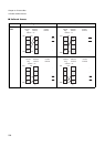
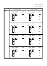
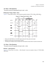
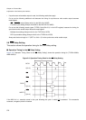
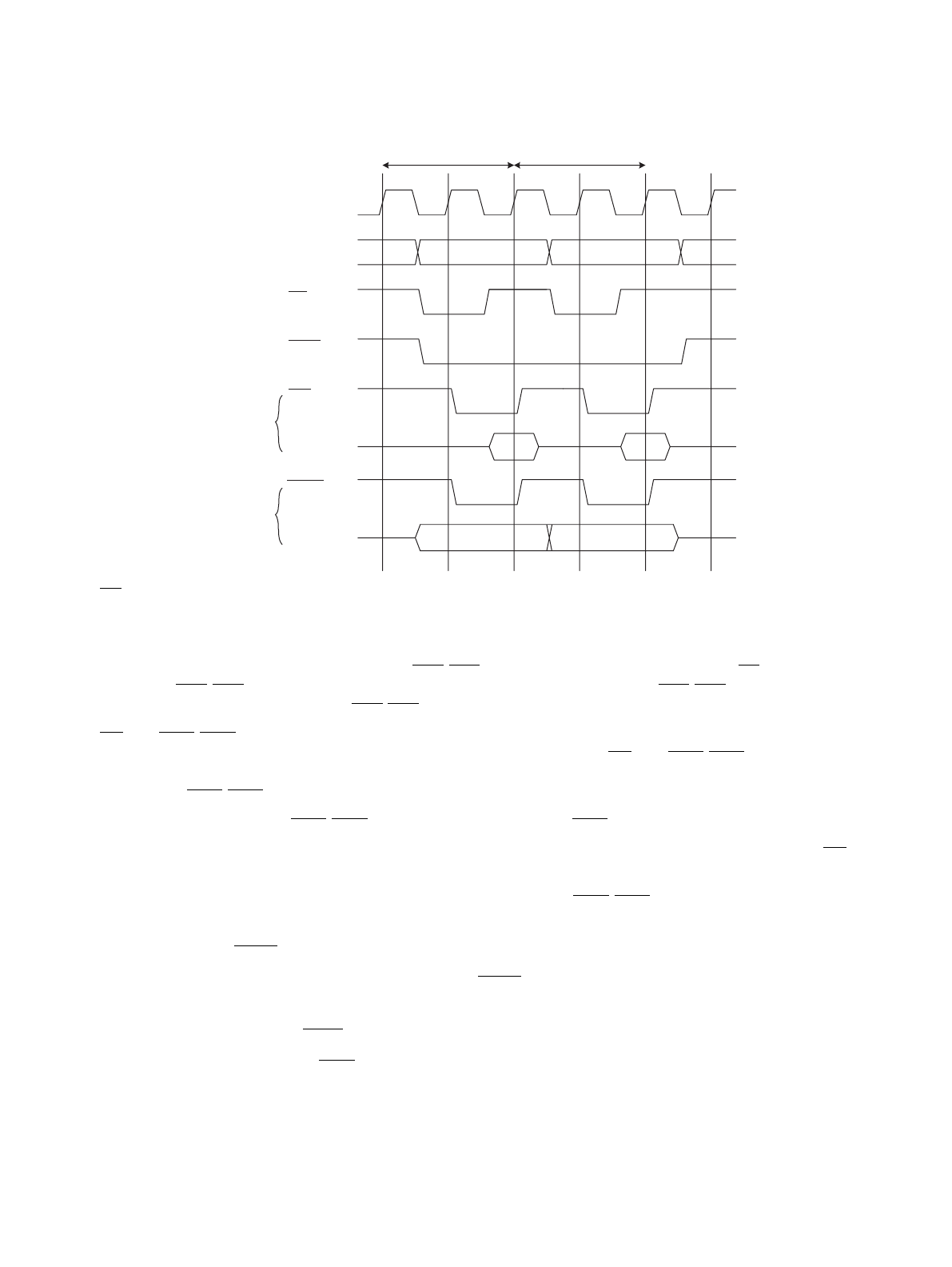
5.2 Operation of WRn + Byte Control Type
This section shows the operation timing for the
WRn + byte control type.
■ Operation Timing of the WRn + Byte Control Type
Figure 5-2 "Timing Chart for the WRn + Byte Control Type" shows the operation timing for (TYP3-0 = 0010
B
,
AWR = 0008
H
).
MCLK
A[31:0]
AS
CSn
RD
D[31:0]
WRn
D[31:0]
READ
WRITE
#1
#2
#1 #2
#1 #2