www.digiembedded.com
107
Working with the CPU
Enabling the caches
On reset, the ICache and DCache entries all are invalidated and the caches disabled.
The caches are not accessed for reads or writes. The caches are enabled using the I,
C, and M bits from the R1: Control register, and can be enabled independently of one
another. Table 43 gives the I and M bit settings for the ICache, and the associated
behavior.
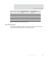
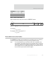
Table 44 shows the page table C bit settings for the ICache (R1 I bit = M bit = 1).
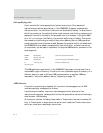
Table 45 gives the R1: Control register C and M bit settings for DCache, and the
associated behavior.
R1 I bit R1 M bit ARM926EJ-S behavior
0 ----- ICache disabled. All instruction fetches are fetched from external memory
(AHB).
1 0 ICache enabled, MMU disabled. All instruction fetches are cachable, with no
protection checks. All addresses are flat-mapped; that is, VA=MVA=PA.
1 1 ICache enabled, MMU enabled. Instruction fetches are cachable or
noncachable, depending on the page descriptor C bit (see Table 44: "Page
table C bit settings for ICache"), and protection checks are performed. All
addresses are remapped from VA to PA, depending on the page entry; that is,
the VA is translated to MVA and the MVA is remapped to a PA.
Table 43: R1:Control register I and M bit settings for ICache
Page table C
bit Description ARM926EJ-S behavior
0 Noncachable ICache disabled. All instruction fetches are fetched from external
memory.
1 Cachable Cache hit Read from the ICache.
Cache miss Linefill from external memory.
Table 44: Page table C bit settings for ICache
R1 C bit R1 M bit ARM926EJ-S behavior
0 0 DCache disabled. All data accesses are to the external memory.
Table 45: R1: Control register I and M bit settings for DCache


