www.digiembedded.com
151
Memory Controller
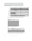
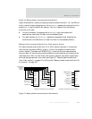
Figure 56: Memory banks constructed from 8-bit memory
Figure 56 shows 8-bit memory configuring memory banks that are 8-, 16-, and 32-bits
wide. In each of these configurations, the
BLSOUT[3:0]_n signals are connected to write
enable (
WE_n) inputs of each 8-bit memory. The WEOUT signal from the memory
controller is not used.
For write transfers, the appropriate BLSOUT[3:0]_n byte lane signals are
asserted low, and direct the data to the addressed bytes.
For read transfers, all BLSOUT[3:0]_n signals are deasserted high, enabling the
external bus to be defined for at least the width of the accessed memory.
Memory banks constructed from 16-or 32-bit memory devices
For memory banks constructed from 16- or 32-bit memory devices, it is important
that the byte lane select (PB) bit is set to 1 within the respective memory bank
control register. This asserts all BLSOUT[3:0]_n lines low during a read access as,
during a read, all device bytes must be selected to avoid undriven byte lanes on the
read data value. With 16- and 32-bit wide memory devices, byte select signals exist
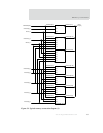
and must be appropriately controlled; see Figure 57, "Memory banks constructed
from 16-bit memory," on page 151 and Figure 58, "Memory banks constructed from 32-
bit memory," on page 152.
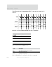
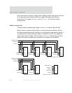
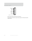
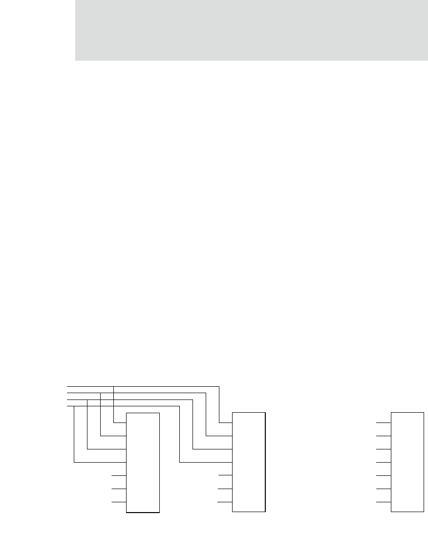
Figure 57: Memory banks constructed from 16-bit memory
32-bit bank consisting of two 16-bit devices 16-bit bank consisting of one 16-bit device
A[20:0]
CE_n
OE_n
WE_n
IO[15:0]
BLSOUT[0]_n
DATA[15:0]
OEOUT_n
ADDROUT[20:0]
STCSOUT_n
LB_n
UB_n
WEOUT_n
BLSOUT[1]_n
A[20:0]
CE_n
OE_n
WE_n
IO[15:0]
BLSOUT[2]_n
DATA[31:16]
LB_n
UB_n
BLSOUT[3]_n
OEOUT_n
ADDROUT[20:0]
STCSOUT_n
WEOUT_n
A[20:0]
CE_n
OE_n
WE_n
IO[15:0]
BLSOUT[0]_n
DATA[15:0]
LB_n
UB_n
BLSOUT[1]_n


