Registers
584
NS9750 Hardware Reference
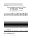
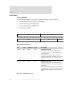
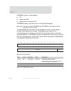
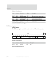
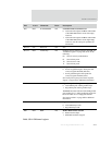
Register bit assignment
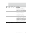
Bits Access Mnemonic Reset Description
D31:27 N/A Reserved N/A N/A
D26 R/W BCD 0x0 Bypass pixel clock divider
Set this field to 1 to bypass the pixel clock divider
logic.
Used primarily for TFT displays.
D25:16 R/W CPL 0x000 Clocks per line
Specifies the number of actual
CLCP clocks to the
LCD panel on each line. This is the number of pixels-
per-line divided by 1 (TFT), 4 or 8 (mono STN), or 2
2/3 (color STN), minus one.
Be sure this value is programmed properly, in addition
to PPL; otherwise, the LCD controller does not work
correctly.
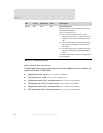
D15 N/A Reserved N/A N/A
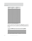
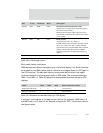
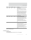
D14 R/W IOE 0x0 Invert output enable
0
CLAC output pin is active high in TFT mode
1
CLAC output pin is active low in TFT mode
Selects the active polarity of the output enable signal
in TFT mode. In this mode, the
CLAC pin is used as an
enable that indicates to the LCD panel when valid
display data is available.
In TFT mode, data is driven onto the LCD data lines
at the programmed edge of
CLCP when CLAC is in its
active state.
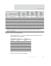
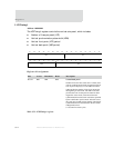
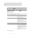
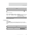
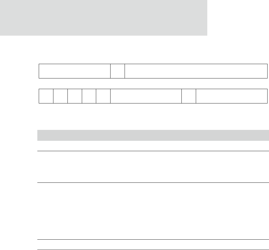
Table 353: LCDTiming2 register
IPC IHS IVS ACB Rsvd PCD
13121110987654321015
14
Rsvd IOE
31 29 28 27 26 25 24 23 22 21 20 19 18 17 1630
BCD CPL
Reserved


