


Static memory controller
136
NS9750 Hardware Reference
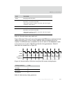
Static memory write control
Write enable programming delay
The delay between the assertion of the chip select and the write enable is
programmable from 1 to 16 cycles using the
WA IT WE N bits of the Static Memory Write
Enable Delay (StaticWaitWen[3:0]) registers. The delay reduces the power
consumption for memories. The write enable is asserted on the rising edge of HCLK
after the assertion of the chip select for zero wait states. The write enable is always
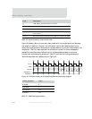
WAITWR N/A
WAITWEN N/A
WAITTURN N/A
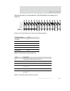
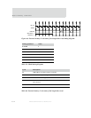
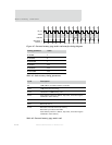
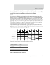
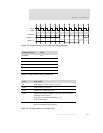
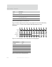
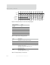
Cycle Description
T0 AHB address provided to memory controller.
T0-T1 AHB transaction processing.
T1-T4 Arbitration of AHB memory ports.
T4-T5 Static memory transfer m0, address, chip select, and control signals
submitted to static memory.
T5-T6 Static memory transfer 1, address, chip select, and control signals
submitted to static memory. Read data byte 0 returned from static
memory.
T6-T7 Static memory transfer 2, address, chip select, and control signals
submitted to static memory. Read data byte 1 returned from the static
memory.
T7-T8 Static memory transfer 3, address chip select, and control signals
submitted to static memory. Read data byte 2 returned from the static
memory.
T8-T9 Read data byte 3 returned from the static memory.
Read data 32-bit word is provided to the AHB.
Table 64: External memory 32-bit burst read from 8-bit memory
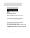
Timing parameters Value
Table 63: Static memory timing parameters