Power sequencing
794
NS9750 Hardware Reference
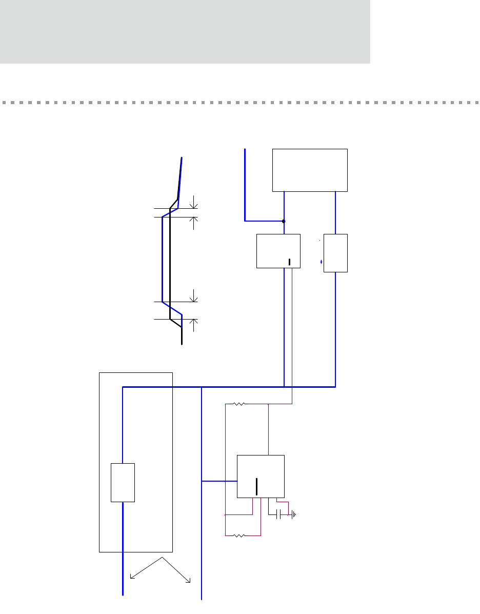
Power sequencing
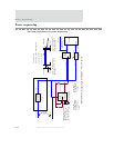
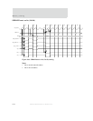
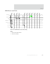
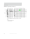
Use these requirements for power sequencing:
VDD
U3
RESET delay is determined
by capacitor on Ct.
Td = 2.1 x 10,0000 x Ct
Td = sec.; Ct = farads
Ct = 0.22uF = 4.6ms delay
I/O
3.3V Power Monitor
2.4K
EN
RESET
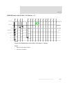
A to B = 1.5V at 80%, or above,
preceeds 3.3V at 80%, or above,
by 1 -100 ms
Ramp-Down
OR
NS9750 Power Sequencing Block Diagram - 5V or 3V source
LT1963AEQ-1.5
Ramp-Up
TPS2022
1 Amp
SENSE
Peripherals connected
to NS9750 I/O
TI LTC7733
A
D
Power
Switch
DC/DC
C
Power Down:
Monitor turns off
3.3V I/O before
1.5V drops.
3.3V_IN
10K
U4
B
LT1765
RESIN
3.3V Source
A = 3.3V_IN at 2.0V
B = 3.3V_IN at 2.93V + Td (RESET delay)
C = 3.3V_IN at 2.93V
D = 3.3V_IN at 2.0V
Regulator
1.0W
Max.
C to D = 1.5V maintained at
80%, or above, until 3.3V
reaches 80% or below.
Power Up:
3.3V I/O is held off
by monitor so that
1.5V core comes
up first.
3.3V_IN
3.3V
5.0V Source
NS9750
LDO
CT
A to B
1.5V
Regulator
U1
CONTROL
Ct
C to D
CORE
3.3V_PERPH
1.5V
Sense = 2.93V
5V/3.3V @ 2.5A
U2
3.3V3.3V_IN
JA = 30 C/W


