


www.digiembedded.com
661
Serial Control Module: SPI
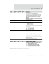
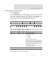
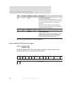
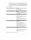
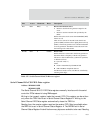
Register bit assignment
Bits Access Mnemonic Reset Description
D31 R/W EBIT 0 Bit-rate generator enable
Enables the internal bit-rate generator when set
to 1.
D30 R/W TMODE 0 Timing mode
Must be set to 1. Use the additional timing configuration
provided by the TDCR and RDCR fields (D[20:19] and
D[18:17] in this register) to configure the channel for 1x,
8x, 16x, or 32x mode.
D29 R/W RXSRC 0 Receive timing source
0 Internal
1 External (input using GPIO pin)
Controls the source of the receiver clock. The receive
clock can be provided by an internal source selected using
the RICS field (see D15).
As an alternative, the receiver clock can be provided by an
input on GPIO pins gpio[6], gpio[14], gpio[22], and
gpio[26] for serial ports B, A, C, and D, respectively.
For SPI master and slave, set to 0 for internal.
D28 R/W TXSRC 0 Transmit clock source
0 Internal
1 External (input using GPIO pin)
Controls the source of the transmitter clock. The
transmitter clock can be provided by an internal source
selected using the TICS field (see D16).
As an alternative, the transmitter clock can be provided by
an input on GPIO pins gpio[7], gpio[15], gpio[23], and
gpio[27] for serial ports B, A, C, and D, respectively.
For SPI master and slave, set to 0 for internal.
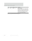
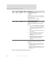
D27 R/W RXEXT 0 Drive receive clock external
0 Disable
1 Enable
Enables the receiver clock to be driven on GPIO pins
gpio[6], gpio[14], gpio[22], and gpio[26] for serial ports
B, A, C, and D, respectively.
For SPI master and slave, set to 0 to disable.
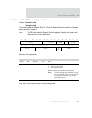
Table 387: Serial Channel B/A/C/D Bit-rate register