www.digiembedded.com
23
NS9750 Pinout
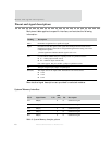
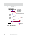
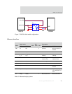
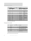
clk_en[3:0] O SDRAM clock enable. Used for SDRAM devices.
Note: The clk_en signals are associated with the dy_cs_n signals.
Connect SDRAM clock enables directly to a 3.3V or pullup resistor to
avoid an SDRAM lockup condition during a manual or brownout
condition reset.
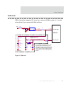
As an alternative, you can use an analog switch to connect the clock
enables to the SDRAM devices to a pullup resistor until the NS9750 device
reset is complete, as indicated by a high level on the reset_done output. See
the sample circuit shown in Figure 7, "NS9750 clock enable
configuration," on page 25.
clk_out[3:1] O SDRAM clocks. Used for SDRAM devices.
clk_out[0] O SDRAM clk_out[0] is connected to clk_in[0].
data[31:0] I/O Read data from memory. Used for the static memory controller and the
dynamic memory controller.
data_mask[3:0] O Data mask output to SDRAMs. Used for SDRAM devices.
clk_in[3:1] I Feedback clocks. Used for SDRAM devices.
clk_in[0] I Feedback clock [0]. Always connects to clk_out[0].
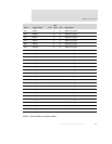
byte_lane_sel_n[3:0] O Static memory byte_lane_select, active low, or write_enable_n for byte-
wide devices.
cas_n O Column address strobe. Used for SDRAM devices.
dy_cs_n[3:0] O SDRAM chip selects. Used for SDRAM devices.
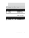
st_oe_n O Output enable for static memories. Used for static memory devices.
ras_n O Row address strobe. Used for SDRAM devices.
st_cs_n[3:0] O Static memory chip selects. Default active low. Used for static memory
devices.
we_n O Write enable. Used for SDRAM and static memories.
ta_strb I Slow peripheral transfer acknowledge can be used to terminate static
memory cycles sooner than the number of wait states programmed in the
chip select setup register.
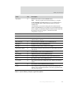
Name I/O Description
Table 4: System Memory interface signal descriptions


