Pinout and signal descriptions
40
NS9750 Hardware Reference
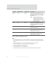
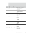
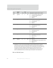
AD2 gpio[44]
1
U 4 I/O 00 Ser port D TxData / SPI port D dout
01 1284 Select (peripheral-driven)
02 LCD data bit 20
03 GPIO 44
AE1 gpio[45] U 4 I/O 00 Ser port D RxData / SPI port D din
01 1284 nStrobe (host-driven)
02 LCD data bit 21
03 GPIO 45
AB3 gpio[46] U 4 I/O 00 Ser port D RTS
01 1284 nAutoFd (host-driven)
02 LCD data bit 22
03 GPIO 46
AA4 gpio[47] U 4 I/O 00 Ser port D CTS
01 1284 nInit (host-driven)
02 LCD data bit 23
03 GPIO 47
AC2 gpio[48] U 2 I/O 00 Timer 14
01 1284 nSelectIn (host-driven)
02 DMA ch 2 req
03 GPIO 48
AD1 gpio[49]
1
U 2 I/O 00 Timer 15
01 1284 peripheral logic high (peripheral-driven)
02 DMA ch 2 done
03 GPIO 49
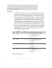
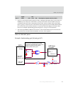
1 This pin is used for bootstrap initialization (see Table 168, “Configuration pins — Bootstrap
initialization,” on page 273). Note that the GPIO pins used as bootstrap pins have a defined
powerup state that is required for the appropriate NS9750 configuration. If these GPIO pins are
also used to control external devices (for example, power switch enable), the powerup state for the
external device should be compatible with the boostrap state. If the powerup state is not
compatible with the bootstrap state, either select a different GPIO pin to control the external
device or add additional circuitry to reach the proper powerup state to the external device.
Pin #
Signal
name
U/D
OD
(mA)
I/O Description (4 options: 00, 01, 02, 03)
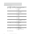
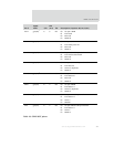
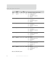
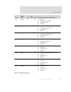
Table 10: GPIO MUX pinout


