www.digiembedded.com
41
NS9750 Pinout
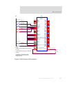
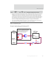
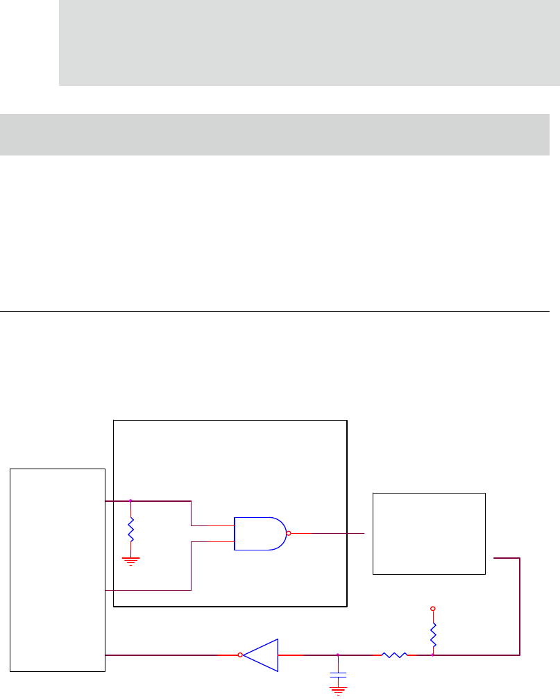
Example: Implementing gpio[16] and gpio[17]
2 gpio[17] is used as both a bootstrap input pin for PLL_ND and an output that controls a power switch for
USB Host power. If the power switch needs to powerup in the inactive state, the enable to the power
switch must be the same value as the bootstrap value for PLL_ND; for example, if PLL_ND requires
high on gpio[17], a high true power switch must be selected. gpio[16] is used for USB_OVR and should
have a noise filter to prevent false indications of overcurrent, unless the USB power IC has this filter
built in. See "Example: Implementing gpio[16] and gpio[17]" on page 41 for an illustration.
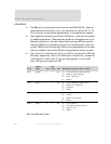
3 The nFault signal GPIO6 or GPIO16 can be used as a code-controlled direction pin for the transceiver.
The polarity cannot be altered inside the NS9750; an inverter will be required.
Pin #
Signal
name
U/D
OD
(mA)
I/O Description (4 options: 00, 01, 02, 03)
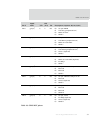
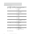
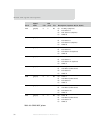
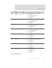
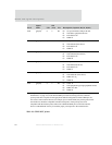
Table 10: GPIO MUX pinout
O
USB Power
Controller
2.4K
NS97xx
INV
GPIO[xy]
Rpull-up
RC filter = 500uS
Cfilter
Rfilter
NAND2
ENABLE_n
OVERCUR_n
3.3V
This circuit is required to prevent USB
power being enabled before code has set
GPIO[17] to mode 00. Pulling down
GPIO[17] effects CPU speed.
USB_PWR,
GPIO[17],
BOOTST_ND4
USB_OVR
GPIO[16]
O


