Static memory controller
128
NS9750 Hardware Reference
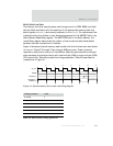
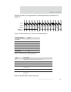
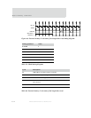
Figure 44 shows external memory read transfers with zero wait states (WA IT RD =0 ).
These transfers can be non-sequential transfers or sequential transfers of a specified
burst length. Bursts of unspecified length are interpreted as INCR4 transfers. All
transfers are treated as separate reads, so have the minimum of five AHB cycles
added.
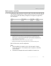
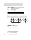
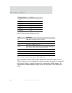
Timing parameter Value
WAITRD 2
WAITOEN 2
WAITPAGE N/A
WAITWR N/A
WAITWEN N/A
WAITTURN N/A
Table 53: Static memory timing parameters
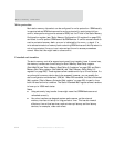
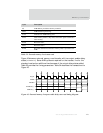
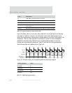
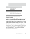
Cycle Description
T0 AHB address provided to memory controller.
T0-T1 AHB transaction processing.
T1-T4 Arbitration of AHB memory ports.
T4-T5 Static memory address, chip select, and control signals submitted to
static memory. Static memory output enable inactive.
T5-T6 Static memory output enable inactive.
T6-T7 Static memory output enable active.
T7-T8 Read data returned from static memory. Data is provided to the AHB.
Table 54: External memory 2 output enable delay state


