www.digiembedded.com
147
Memory Controller
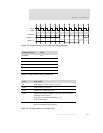
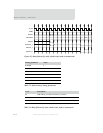
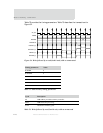
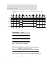
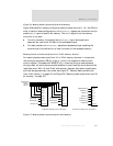
Figure 55 shows a zero wait read followed by a zero wait write with two turnaround
cycles added. The standard minimum of three AHB arbitration cycles are added to
the read transfer and two wait states are added to the write transfer (as for any
read-write transfer sequence).
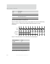
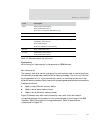
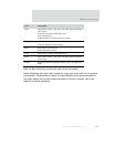
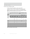
T4-T5 Static memory address, chip select, and control signals submitted to
static memory.
Write data is read from AHB memory port.
Write enable inactive.
AHB read address provided to memory controller.
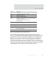
T5-T6 Write enable taken active.
Write data submitted to static memory.
T6-T7 Static memory writes the data.
Write enable taken inactive.
T7-T8 Static memory control signals taken inactive.
T8-T9 Static memory address, chip select, and control signals submitted to
static memory.
T9-T10 Read data returned from the static memory. Data is provided to the
AHB.
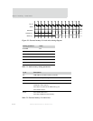
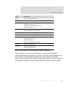
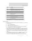
Cycle Description
Table 76: Write followed by read (both 0 wait) with no turnaround


