www.digiembedded.com
493
BBus Bridge
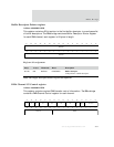
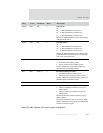
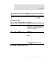
D24:23 R/W SB 0 Source burst
00 1
01 2 (Recommended for 8-bit devices)
10 4 (Recommended for 16-bit devices)
11 8 (Recommended for 32-bit devices)
Defines the AHB maximum burst size allowed when
reading from the source.
D22:21 R/W DB 0 Destination burst
00 1
01 2 (Recommended for 8-bit devices)
10 4 (Recommended for 16-bit devices)
11 8 (Recommended for 32-bit devices)
Defines the AHB maximum burst size when writing
to the destination. This field must be set to the same
value as the source burst field.
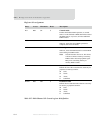
D20 R/W SINC_N 0 Source address increment
0 Increment source address pointer
1 Do not increment source address pointer
Controls whether the source address pointers are
incremented after each DMA transfer.
D19 R/W DINC_N 0 Destination address increment
0 Increment destination address pointer
1 Do not increment destination address pointer
Controls whether the destination address pointers are
incremented after each DMA transfer.
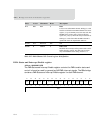
D18:16 R/W POL 0 Always set this field to 0.
D17 R/W MODE 0 Fly-by mode
0 Defines a peripheral to memory fly-by write
DMA transfer
1 Defines a memory-to-peripheral fly-by read
DMA transfer
Defines the direction of data movement for fly-by
DMA transfers.
This field is not used for memory-to-memory DMA
transfers initiated by writing the CG field in the DMA
Channel 1/2 Control register.
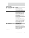
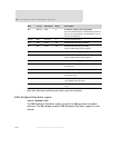
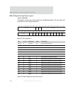
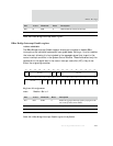
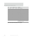
Bit(s) Access Mnemonic Reset Description
Table 297: DMA Channel 1/2 Control register bit definition


