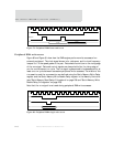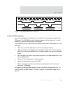
Two-channel AHB DMA controller (AHB bus)
482
NS9750 Hardware Reference
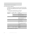
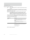
Static RAM chip select configuration
The AHB DMA controller accesses an external peripheral using the external memory
bus and one of the static RAM chip select signals (st_cs_n[N]). This table describes
how to program the static RAM chip select control registers for access using the AHB
DMA controller.
Fields not explicitly listed should be left in the reset state.
Fields listed but not defined must be defined by the user.
Register Name Field Value Comment
Configuration PB 1 System requirement.
PM user defined Set to 1 if it is not necessary for the chip select
signal to toggle for each access.
MW user defined N/A
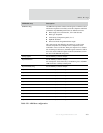
Read Delay WTRD user defined Compute the total delay using the equation
provided in "Peripheral DMA read access" on
page 477. The total delay should be divided by
the AHB clock period to produce this value.
Round up any fractional result.
Page Read Delay WTPG user defined For most applications, this value will be the same
as the value for WTRD.
Output Enable Delay WOEN user defined If the
ACK signal is used to initiate a peripheral
read, this field should be set
to 0.
If signal
st_oe_n is used to initiate a peripheral
read, this field should be set to (at least) 1.
Write Enable Delay WWEN user defined For most applications, this field can be left in the
default state.
Write Delay WTWR user defined For most applications, this field can be left in the
default state.
Turn Delay WTTN user defined For most applications, this field can be left in the
default state.
Table 290: Static RAM chip select configuration


