Registers
226
NS9750 Hardware Reference
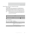
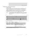
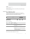
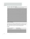
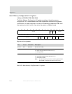
Table 157 shows address mapping for the Dynamic Memory Configuration 0-3
registers. Address mappings that are not shown in the table are reserved.
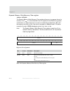
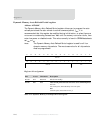
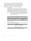
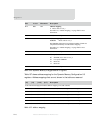
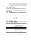
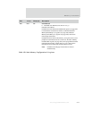
D14 R/W AM Address mapping
0 Reset value on
reset_n
See Table 157, “Address mapping,” on page 226 for more
information.
D13 N/A Reserved N/A (do not modify)
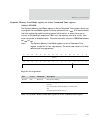
D12:07 R/W AM1 Address mapping
00000000 Reset value on
reset_n
The SDRAM column and row width and number of banks are
computed automatically from the address mapping.
See Table 157, “Address mapping,” on page 226 for more
information.
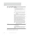
D06:05 N/A Reserved N/A (do not modify)
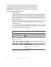
D04:03 R/W MD Memory device
00 SDRAM (reset value on
reset_n)
01 Low-power SDRAM
10 Reserved
11 Reserved
D02:00 N/A Reserved N/A (do not modify)
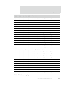
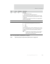
[14] [12] [11:9] [8:7] Description
16-bit external bus high-performance address mapping (row, bank column)
0 0 000 00
16 Mb (2Mx8), 2 banks, row length=11, column length=9
0 0 000 01
16 Mb (1Mx16), 2 banks, row length=11, column length=8
0 0 001 00
64 Mb (8Mx80, 4 banks, row length=12, column length=9
0 0 001 01
64 Mb (4Mx16), 4 banks, row length=12, column length=8
0 0 010 00
128 Mb (16Mx8), 4 banks, row length=12, column length=10
0 0 010 01
128 Mb (8Mx16), 4 banks, row length=12, column length=9
Table 157: Address mapping
Bits Access Mnemonic Description
Table 156: Dynamic Memory Configuration 0–3 registers


