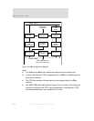
Two-channel AHB DMA controller (AHB bus)
478
NS9750 Hardware Reference
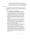
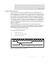
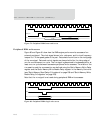
Figure 79: Peripheral DMA burst read access
Peripheral DMA write access
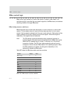
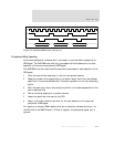
Figure 80 and Figure 81 show how the DMA engine performs write accesses of an
external peripheral. The clock signal shown is for reference, and its clock frequency
is equal to 1/2 the speed grade of the part. Data should be written on the rising edge
of the
WE# signal. Data and control signals are always held after the rising edge of
WE# for one reference CLK cycle. The CS# signal is guaranteed to be deasserted for at
least one
CLK cycle between successive peripheral write accesses. The widths of the
CS# assertion and the WE# assertion are defined using the Static Memory Write Delay
register and the Static Memory Write Enable Delay register in the Memory Controller
(see "Static Memory Read Delay 0–3 registers" on page 236 and "Static Memory Write
Enable Delay 0–3 registers" on page 234).
Note that the
ACK signal is not used during peripheral DMA write accesses.
Figure 80: Peripheral DMA single write access
READ_EN
DQ
CS#
CLK
DATA0
DATA1
DQ
CS#
CLK
WE#
Data Valid


