www.digiembedded.com
529
BBus Utility
GPIO Control registers
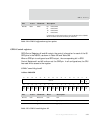
GPIO Control Registers #1 and #2 contain the control information for each of the 50
GPIO pins in the NS9750, as shown in Table 325 and Table 326.
When a GPIO pin is configured as a GPIO output, the corresponding bit in GPIO
Control Registers #1 and #2 is driven out the GPIO pin. In all configurations, the CPU
has read/write access to the register.
GPIO Control Register#2
Address: 9060 0034
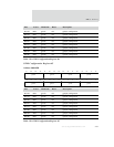
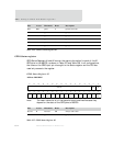
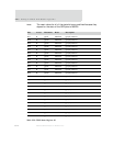
D01:00 R/W PINn 00 Function #0
01 Function #1
10 Function #2
11 Function #3
Use these bits to select the function to use. See the discussion of GPIO
MUX for details about the available pin functions.
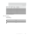
Bits Access Mnemonic Description
Table 324: GPIO Configuration register options
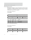
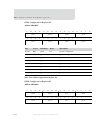
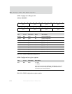
Bits Access Mnemonic Reset Description
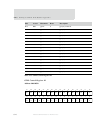
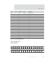
D31:18 N/A Reserved N/A N/A
D17 R/W gpio49 0 gpio[49] control bit
D16 R/W gpio48 0 gpio[48] control bit
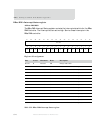
Table 325: GPIO Control Register #2
13121110987654321015 14
31 29 28 27 26 25 24 23 22 21 20 19 18 17 1630
gpio
49
Reserved
gpio
48
gpio
47
gpio
46
gpio
45
gpio
44
gpio
43
gpio
42
gpio
41
gpio
40
gpio
39
gpio
38
gpio
37
gpio
36
gpio
35
gpio
34
gpio
33
gpio
32


