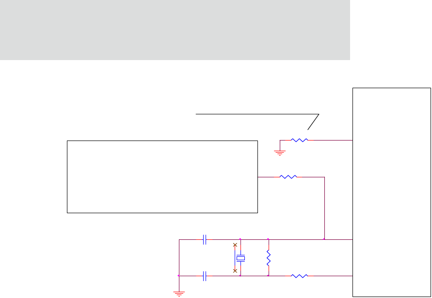
System clock
14
NS9750 Hardware Reference
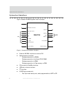
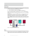
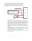
Figure 4: System clock
The PLL parameters are initialized on powerup reset, and can be changed by
software from f
max
to 1/2 f
max
. For a 200 MHz grade, then, the CPU may change from
200 MHZ to 100 MHz, the AHB system bus may change from 100 MHz to 50 MHz, and
the peripheral BBus may change from 50 MHz to 25 MHz. If changed by software, the
system resets automatically after the PLL stabilizes (approximately 4 ms).
The system clock provides clocks for CPU, AHB system bus, peripheral BBus, PCI/
CardBus, LCD, timers, memory controller, and BBus modules (serial modules and 1284
parallel port).
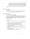
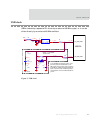
The Ethernet MAC uses external clocks from a MII PHY or a RMII PHY. For a MII PHY,
these clocks are input signals:
rx_clk on pin T3 for receive clock and tx_clk on pin V3 for
transmit clock. For a RMII, there is only one clock, and it connects to the
rx_clk on pin
T3. In this case, the transmit clock,
tx_clk, should be tied low.
PCI/CardBus, LCD controller, serial modules (UART, SPI), and 1284 port can optionally
use external clock signals.
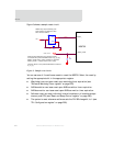
C19
10pF
S_PLL_BP_
GPIO19_PLL_BP
C20
10pF
X2
20-40MHz
X1_SYS
X2_XTAL
X1_SYS_OSC is qualified for an external LVTTL clock up to
400 MHz in PLL bypass mode. The system PLL is bypassed
by pulling down GPIO19. In PLL bypass mode, the ARM9
CPU is ½ the frequency of X!_SYS_OSC.
When the PLL is enabled, the clock input range is 20 - 40
MHz.
X1_SYS_OSC
Add R10 to bypass SYS PLL
R12
1M
R11
100
X2_SYS
R10
2R4K
R13
330 OHM
NS9750
X2_SYS_OSC


