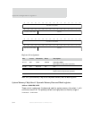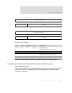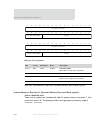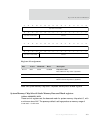
System configuration registers
300
NS9750 Hardware Reference
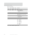
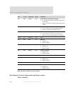
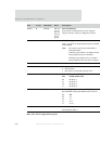
D20:16 R PLLND
HW strap
gpio[17],
gpio[12],
gpio[10],
gpio[8],
gpio[4]
PLL ND status[4:0]
Status register to determine the powerup strapping
settings or the new settings as changed by software.
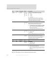
D15 W PLLSW 0x0 PLL SW change
Write a 1 to this bit to change the PLL settings as defined
in bits D09:00.
Note: The system is held in reset until the PLL is
locked and settled.
If the PLL bypass SW bit is set (D09), the PLL
setting change and reset is immediate.
If the PLL bypass SW bit is not set, the PLL
setting change and reset take 4ms to complete.
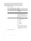
D14:10 N/A Reserved N/A N/A
D09 R/W PLLBW 0x0 PLL bypass SW
0 PLL operation
1 PLL bypass; use the input reference clock
D08:07 R/W FSEL 0x0 PLL frequency select (FS) [1:0]
PLL Output divider value
00 Divide by 1
01 Divide by 2
10 Divide by 4
11 Divide by 8
D06:05 R/W CPCC 0x3 PLL charge pump current control (IS) [1:0]
Recommended settings determined by ND, as follows:
IS ND
00 0–3
01 4–7
10 8–15
11 16–31
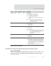
D04:00 R/W NDSW 0x1A PLL ND SW [4:0]
PLL multiplier (ND+1).
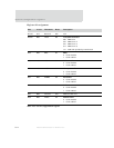
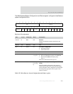
Bits Access Mnemonic Reset Description
Table 188: PLL Configuration register


