www.digiembedded.com
31
NS9750 Pinout
PCI/CardBus signals
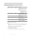
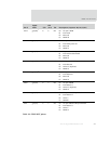
Most of the CardBus signals are the same as the PCI signals. Other CardBus signals are
unique and multiplexed with PCI signals for the NS9750. Table 9 shows these unique
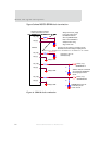
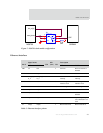
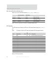
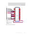
signals. Figure 8 illustrates how to terminate an unused PCI.
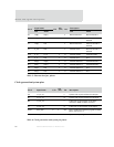
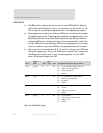
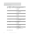
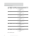
AD22 pci_int_d_n
2
N/A I PCI interrupt request D
AE26 pci_reset_n
3
N/A I/O PCI reset, output if internal central resource
enabled
AB24 pci_clk_in U N/A I PCI clock in. (Connected to pci_clk_out or an
externally generated PCI reference clock.)
AA23 pci_clk_out N/A O PCI clock out
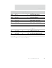
PCI signal CardBus signal CardBus type Description
INTA# CINT#
4
Input CardBus interrupt pin. The INTA2PCI pin in the
PCI Miscellaneous Support register must be set
to 0.
INTB# CCLKRUN#
4
Bidir CardBus pin used to negotiate with the external
CardBus device before stopping the clock.
Allows external CardBus device to request that
the clock be restarted.
INTC# CSTSCHG
5
Input CardBus status change interrupt signal.
GNT1# CGNT#
4
Output Grant to external CardBus device from
NS9750’s internal arbiter.
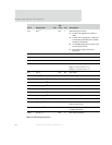
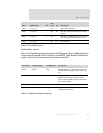
Table 9: CardBus IO multiplexed signals
Pin # Signal name U/D
OD
(mA)
I/O Description
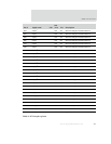
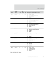
Table 8: PCI interface pinout


