www.digiembedded.com
141
Memory Controller
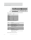
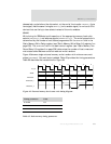
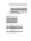
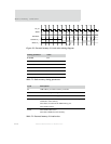
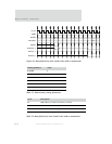
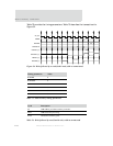
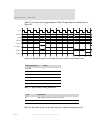
Figure 52 shows two external memory write transfers with zero wait states
(
WA IT WR =0). Four AHB wait states are added to the second write, because this write
can be started only when the first write has completed. This is the timing of any
sequence of write transfers, nonsequential to nonsequential or nonsequential to
sequential, with any value of
HBURST. The maximum speed of write transfers is
controlled by the external timing of the write enable relative to the chip select, so
all external writes must take two cycles to complete: the cycle in which write enable
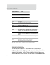
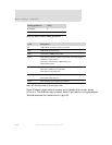
is asserted and the cycle in which write enable is deasserted. Table 71 provides the
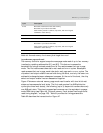
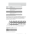
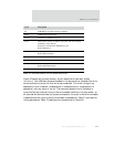
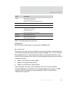
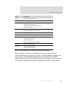
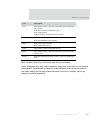
timing parameters. Table 72 describes the transactions for Figure 52.
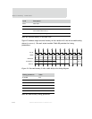
Cycle Description
T0 AHB address provided to memory controller.
T0-T1 AHB transaction processing.
T1-T4 Arbitration of AHB memory ports.
T4-T5 Static memory transfer 0, address, chip select, and control signals
submitted to static memory.
Write data is read from the AHB memory port.
Write enable active.
T5-T6 Write data submitted to static memory.
Write enable wait state 1.
T6-T7 Write enable wait state 2.
T7-T8 Write enable taken active.
T8-T9 Static memory writes the data.
Write enable taken inactive.
T9-T10 Static memory control signals taken inactive.
Table 70: External memory 2 write enable delay write


